


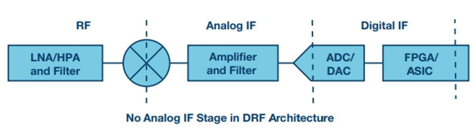
Figure 1 is a block diagram of a typical transmitter and receiver.
RF-class processing RF signals, in the current LTE standard, the signal frequency range is generally 700 MHz to 3.8 GHz. Through the mixer, modulator or demodulator - these are the mixing unit - after processing, the RF signal moves to a lower frequency of DC to 300 MHz below.The processing module from the data converter to the mixer consists of a converter (ADC or DAC), an analog filter and an intermediate frequency amplifier, which we can refer to as an analog intermediate frequency stage.
After the converter (actually after the quantizer part of the converter), the signal becomes a digital signal; it is called the digital IF stage along with the subsequent FPGA or ASIC. For each digital signal processing module in this stage, it is commonly referred to as DUC (digital upconverter) in the Tx path and is commonly referred to as DDC (digital downconverter) in the Rx path.Direct RF architecture is an exception, where the data converter directly to the RF signal sampling, and therefore no analog IF stage, the signal chain only by the radio frequency and digital frequency level composition.
Typical DDC modules include carrier selection, downconverter, filter and extractor. These functional blocks operate in sequence, or can be bypassed separately, resulting in a complex signal or a real signal at DC, depending on the requirements of the subsequent FPGA or ASIC (whose sampling rate is low).
Typical DUC modules include interpolation, filters, upconverter, and carrier combiner. According to the system architecture design, DUC generates a complex signal or intermediate frequency signal located at DC, or generates radio frequency signal directly. The processing of DUC is almost the opposite of that of DDC.Often multiple DDC and DUC levels are cascaded to provide flexibility. Independent DDCs and DUCs need to process multiple carriers in parallel, after which the output signals are output or separated in the received signal.
DDC
The Rx link requires a higher sampling rate to avoid aliasing of the signal, simplifying the analog filter design, and providing a wider signal band. On the other hand, in order to save power, cost and high-speed logic in FPGA / ASIC, it is best to reduce the data rate on the interface. The integrated DDC of the converter will address the above requirements.
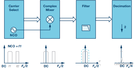
Figure 2 is a block diagram of a typical DDC.
NCO and mixer
In order to select the desired carrier from the interference (blocking signal and other carriers), the output frequency of the NCO is mixed with the input IF signal to shift the desired carrier frequency to DC. This reduces the complexity of subsequent filtering and extraction levels.
Filtering and extraction
After the NCO and mixing stages, a low-pass filter is used to select the desired filter and suppress other unwanted signals. After the filter, use a 2x extractor to reduce the data rate. In order to save resources and provide flexibility to the customer, the half band FIR filter plus 2 times the extractor is incorporated in a module; re-use the module to cascade three to four. The system designer can choose to use some or all of them according to the application needs. The converter may also provide two times the other extraction rate to provide greater flexibility, especially in the RF ADC.
DUC
The Tx chain has the same requirements as the Rx chain: requires a high sampling rate to simplify the filter design, making the signal frequency at high frequencies or directly into RF, and far pushing the mirror, but the interface wants to use a lower data rate. The integrated DUC of the converter will address these requirements.
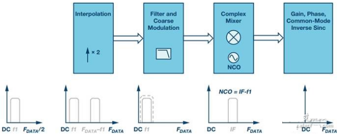
Figure 3 is a block diagram of a typical DUC.
Interpolation and filtering
The simplest digital interpolation algorithm is called "zero padding", that is, between each two samples inserted 0. Sampling rate doubled, but in the resulting spectrum will also produce the frequency of Fs - Fif mirror. Thus, a filter stage is required after the interpolator to eliminate the mirror or raw carrier (depending on the application). If the original carrier is eliminated, the result will be interpolated and Fs / 2 coarse.
As in the DDC, the 2x interpolation and the filter are merged into one module. And then repeat this function module and cascade three to four levels to increase flexibility. Additional interpolation coefficients other than 2 times can be used to provide greater flexibility, especially in RF DACs.
NCO and mixer
The NCO and mixer stages in the DUC are very similar to the same modules in the DDC, but on the contrary, the carrier frequency is shifted to the desired IF or RF frequency, as required by the system architecture. In a zero-frequency architecture, this module can be bypassed to keep the carrier in the DC. The gain, phase, I / Q offset and inverse Sinc gain, phase adjustment, I / Q offset, and inverse sinc module are many IF / RF DAC attachments. The gain, phase adjustment and I / Q offset are often used together to independently tune the output signal I / Q channels to compensate for different types of I / O mismatches (DACs, analog filters and modulators), and finally from analog modulators Output a low signal leakage and low resolution ideal signal. The anti-sinc filter compensates the sinc roll caused by the DAC, which affects flatness and signal amplitude, especially in broadband applications using high frequency or direct RF architectures.