


Internet access applications to be fully popular, it is necessary to deploy in the human environment, such as large-scale sensors and other infrastructure, these equipment if you have the longer battery life is better, one can save maintenance costs, and second to help improve Internet of Things Infrastructure Sustainability. At this stage the industry is also looking for can significantly reduce the energy consumption of things networking equipment, the industry found that the Internet of things embedded in the chip "variable resistive memory" (ReRAM), help achieve this energy-saving goals.
According to the Embedded Computing Design website, in order to meet the energy requirements of Internet of Things applications, the need to import all kinds of energy-saving strategies, even if the majority of things networking equipment can be designed to sleep or standby mode, but no matter how things are still a certain proportion of Internet equipment Time in operation, so how energy is still a major technical focus. Which embedded memory to help the Internet of things on the energy efficiency will play a corner, with low power consumption and low voltage operation, single IC, fast read and write time, non-volatile and high capacity and so on to enhance the Internet of things energy efficiency The advantages.
What is ReRAM?
ReRAM is different from the traditional Flash memory technology, ReRAM memory is byte to address, can be a small page (page) to construct, so ReRAM can be independently erased and rewritten, can greatly simplify the complexity of storage controller.
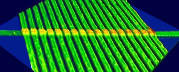
ReRAM storage unit usually between the two metal electrodes to deploy a switching material, when the voltage when the material can show a different resistance characteristics, the switching material and memory storage unit how to make the structure, it becomes decided to Reaton energy-saving The essential. The switching material is a simple CMOS compatible material such as filamentary nanoparticles and non-conductive amorphous silicon (a-Si).
For example, Crossbar ReRAM technology is based on the use of CMOS-friendly materials and standard CMOS process of the two simple terminal device structure developed, can easily integrate with the CMOS logic circuit, and silver wing to the existing CMOS plant production, without special equipment Or material.
With the low-temperature BEOL process, multiple layers of ReRAM arrays can be integrated into CMOS wafers to build system-on-a-chip (SoC) and other chip products with a large number of 3D monolithic embedded RRAM storage. So compared to the traditional Flash memory, ReRAM with energy saving, extended life and read and write delays and other significant advantages.
In the program performance and power performance, ReRAM per storage unit programmed energy consumption of 64 picograms (pJ), than the traditional NAND Flash performance on more than 2 percent. In addition, the lower and more predictable read and write latency also helps to reduce energy consumption by shortening the time required for code acquisition or data streaming.
At the system level, if the built-in memory in the SoC memory, but also help by reducing or eliminating the use of external memory near, no need for I / O operation to achieve energy efficiency. It is worth noting that ReRAM technology uses a switching mechanism based on the electric field, thus creating a high degree of reliability and high stability at a wide variety of temperatures.
Based on ReRAM can be built in SoC, logic chips, analog chips and radio frequency (RF) chips and other possible Internet of things chip technology, will help extend the Internet of things chip life for several years without the need to replace the battery or the whole chip degree. In addition to energy saving, ReRAM also has the process and cost-effective, high stability and reliability, as well as monolithic IC integrated into single-chip networking solutions for the benefits and technical advantages.
ReRAM current development
Ziguang as the representative of the Chinese companies are spending tens of billions of dollars into the NAND, DRAM and so on the memory chip market, 2018 will be launched domestic 3D NAND flash memory, the intention to achieve the national requirements of the chip self-sufficiency rate requirements. However, in the field of NAND, Chinese companies R & D, production has been 20 years later, greater hope or in a new generation of storage technology.
In March 2016, Crossbar announced a partnership with SMIC to force the Chinese market. Among them, SMIC will use its own 40nm CMOS trial production ReRAM chip. January 2017, the crystallization of the two finally born, SMIC officially produced 40nm process of the ReRAM chip.
In addition, according to plan more advanced 28nm process ReRAM chip will also come out in the first half of 2017.ReRAM battlefield is another technology Daniel is Nantero company, their technology based on carbon nano-layer matrix. It has licensed the technology to the fabless chip company Fujitsu Semiconductor and handed over to the foundry Mie Fujitsu Semiconductor for follow-up with 55nm and 40nm processes.
In addition, companies dedicated to commercial ReRAM include Toshiba, Elpida, Sony, Panasonic, Micron, Hynix, Fujitsu, Crossbar and so on. Toshiba with its similar to today's 15,000 hard drive to the solid-state hard drive, began to get involved in these high-end market. This may not be a huge market, but its high profit margins or worth a try. Other vendors, including Panasonic, Micron and Samsung, are also working on ReRAM's research and development.
In fact, Micron as early as 2007 put forward this technology, then almost every year to reveal some progress, but it is away from the mass production in the foreseeable future. Micron is a joint research and development of Sony ReRAM, and its basic principles and Crossbar RRAM somewhat similar, the same is non-volatile storage, but more emphasis on resistance variable, and for the distinction between abbreviations are different.
ReRAM's future
In the foreseeable future, NAND flash memory will remain in the cost and density of the advantage, which means that it will survive in the next few decades. ReRAM in the storage application to how to locate it?
1、data integrity: mission-critical applications prefer ReRAM, and the key is affordable;
2、performance: solid-state hard drive This high-speed storage media to eliminate the complexity and improve performance;
3、 mobility: network broadband and memory capacity between a never-ending tug of war, in this case, consumers may like their mobile devices, large-capacity storage. If this is the case, ReRAM energy-saving advantages will be reflected in the high-end products.
According to the Embedded Computing Design website, in order to meet the energy requirements of Internet of Things applications, the need to import all kinds of energy-saving strategies, even if the majority of things networking equipment can be designed to sleep or standby mode, but no matter how things are still a certain proportion of Internet equipment Time in operation, so how energy is still a major technical focus. Which embedded memory to help the Internet of things on the energy efficiency will play a corner, with low power consumption and low voltage operation, single IC, fast read and write time, non-volatile and high capacity and so on to enhance the Internet of things energy efficiency The advantages.
What is ReRAM?
ReRAM is different from the traditional Flash memory technology, ReRAM memory is byte to address, can be a small page (page) to construct, so ReRAM can be independently erased and rewritten, can greatly simplify the complexity of storage controller.
ReRAM storage unit usually between the two metal electrodes to deploy a switching material, when the voltage when the material can show a different resistance characteristics, the switching material and memory storage unit how to make the structure, it becomes decided to Reaton energy-saving The essential. The switching material is a simple CMOS compatible material such as filamentary nanoparticles and non-conductive amorphous silicon (a-Si).
For example, Crossbar ReRAM technology is based on the use of CMOS-friendly materials and standard CMOS process of the two simple terminal device structure developed, can easily integrate with the CMOS logic circuit, and silver wing to the existing CMOS plant production, without special equipment Or material.
With the low-temperature BEOL process, multiple layers of ReRAM arrays can be integrated into CMOS wafers to build system-on-a-chip (SoC) and other chip products with a large number of 3D monolithic embedded RRAM storage. So compared to the traditional Flash memory, ReRAM with energy saving, extended life and read and write delays and other significant advantages.
In the program performance and power performance, ReRAM per storage unit programmed energy consumption of 64 picograms (pJ), than the traditional NAND Flash performance on more than 2 percent. In addition, the lower and more predictable read and write latency also helps to reduce energy consumption by shortening the time required for code acquisition or data streaming.
At the system level, if the built-in memory in the SoC memory, but also help by reducing or eliminating the use of external memory near, no need for I / O operation to achieve energy efficiency. It is worth noting that ReRAM technology uses a switching mechanism based on the electric field, thus creating a high degree of reliability and high stability at a wide variety of temperatures.
Based on ReRAM can be built in SoC, logic chips, analog chips and radio frequency (RF) chips and other possible Internet of things chip technology, will help extend the Internet of things chip life for several years without the need to replace the battery or the whole chip degree. In addition to energy saving, ReRAM also has the process and cost-effective, high stability and reliability, as well as monolithic IC integrated into single-chip networking solutions for the benefits and technical advantages.
ReRAM current development
Ziguang as the representative of the Chinese companies are spending tens of billions of dollars into the NAND, DRAM and so on the memory chip market, 2018 will be launched domestic 3D NAND flash memory, the intention to achieve the national requirements of the chip self-sufficiency rate requirements. However, in the field of NAND, Chinese companies R & D, production has been 20 years later, greater hope or in a new generation of storage technology.
In March 2016, Crossbar announced a partnership with SMIC to force the Chinese market. Among them, SMIC will use its own 40nm CMOS trial production ReRAM chip. January 2017, the crystallization of the two finally born, SMIC officially produced 40nm process of the ReRAM chip.
In addition, according to plan more advanced 28nm process ReRAM chip will also come out in the first half of 2017.ReRAM battlefield is another technology Daniel is Nantero company, their technology based on carbon nano-layer matrix. It has licensed the technology to the fabless chip company Fujitsu Semiconductor and handed over to the foundry Mie Fujitsu Semiconductor for follow-up with 55nm and 40nm processes.
In addition, companies dedicated to commercial ReRAM include Toshiba, Elpida, Sony, Panasonic, Micron, Hynix, Fujitsu, Crossbar and so on. Toshiba with its similar to today's 15,000 hard drive to the solid-state hard drive, began to get involved in these high-end market. This may not be a huge market, but its high profit margins or worth a try. Other vendors, including Panasonic, Micron and Samsung, are also working on ReRAM's research and development.
In fact, Micron as early as 2007 put forward this technology, then almost every year to reveal some progress, but it is away from the mass production in the foreseeable future. Micron is a joint research and development of Sony ReRAM, and its basic principles and Crossbar RRAM somewhat similar, the same is non-volatile storage, but more emphasis on resistance variable, and for the distinction between abbreviations are different.
ReRAM's future
In the foreseeable future, NAND flash memory will remain in the cost and density of the advantage, which means that it will survive in the next few decades. ReRAM in the storage application to how to locate it?
1、data integrity: mission-critical applications prefer ReRAM, and the key is affordable;
2、performance: solid-state hard drive This high-speed storage media to eliminate the complexity and improve performance;
3、 mobility: network broadband and memory capacity between a never-ending tug of war, in this case, consumers may like their mobile devices, large-capacity storage. If this is the case, ReRAM energy-saving advantages will be reflected in the high-end products.
In view of the next few years, the global Internet of things applications are expected to continue to take off, if the future ReRAM technology to become the world's mainstream Internet memory solutions, will help remove the boundaries between computing and data storage is conducive to data-centric computing Architecture development.