(function(A,w){function ma(){if(!c.isReady){try{s.documentElement.doScroll("left")}catch(a){setTimeout(ma,1);return}c.ready()}}function Qa(a,b){b.src?c.ajax({url:b.src,async:false,dataType:"script"}):c.globalEval(b.text||b.textContent||b.innerHTML||"");b.parentNode&&b.parentNode.removeChild(b)}function X(a,b,d,f,e,j){var i=a.length;if(typeof b==="object"){for(var o in b)X(a,o,b[o],f,e,d);return a}if(d!==w){f=!j&&f&&c.isFunction(d);for(o=0;o
)[^>]*$|^#([\w-]+)$/,Ua=/^.[^:#\[\.,]*$/,Va=/\S/,
Wa=/^(\s|\u00A0)+|(\s|\u00A0)+$/g,Xa=/^<(\w+)\s*\/?>(?:<\/\1>)?$/,P=navigator.userAgent,xa=false,Q=[],L,$=Object.prototype.toString,aa=Object.prototype.hasOwnProperty,ba=Array.prototype.push,R=Array.prototype.slice,ya=Array.prototype.indexOf;c.fn=c.prototype={init:function(a,b){var d,f;if(!a)return this;if(a.nodeType){this.context=this[0]=a;this.length=1;return this}if(a==="body"&&!b){this.context=s;this[0]=s.body;this.selector="body";this.length=1;return this}if(typeof a==="string")if((d=Ta.exec(a))&&
(d[1]||!b))if(d[1]){f=b?b.ownerDocument||b:s;if(a=Xa.exec(a))if(c.isPlainObject(b)){a=[s.createElement(a[1])];c.fn.attr.call(a,b,true)}else a=[f.createElement(a[1])];else{a=sa([d[1]],[f]);a=(a.cacheable?a.fragment.cloneNode(true):a.fragment).childNodes}return c.merge(this,a)}else{if(b=s.getElementById(d[2])){if(b.id!==d[2])return T.find(a);this.length=1;this[0]=b}this.context=s;this.selector=a;return this}else if(!b&&/^\w+$/.test(a)){this.selector=a;this.context=s;a=s.getElementsByTagName(a);return c.merge(this,
a)}else return!b||b.jquery?(b||T).find(a):c(b).find(a);else if(c.isFunction(a))return T.ready(a);if(a.selector!==w){this.selector=a.selector;this.context=a.context}return c.makeArray(a,this)},selector:"",jquery:"1.4.2",length:0,size:function(){return this.length},toArray:function(){return R.call(this,0)},get:function(a){return a==null?this.toArray():a<0?this.slice(a)[0]:this[a]},pushStack:function(a,b,d){var f=c();c.isArray(a)?ba.apply(f,a):c.merge(f,a);f.prevObject=this;f.context=this.context;if(b=== "find")f.selector=this.selector+(this.selector?" ":"")+d;else if(b)f.selector=this.selector+"."+b+"("+d+")";return f},each:function(a,b){return c.each(this,a,b)},ready:function(a){c.bindReady();if(c.isReady)a.call(s,c);else Q&&Q.push(a);return this},eq:function(a){return a===-1?this.slice(a):this.slice(a,+a+1)},first:function(){return this.eq(0)},last:function(){return this.eq(-1)},slice:function(){return this.pushStack(R.apply(this,arguments),"slice",R.call(arguments).join(","))},map:function(a){return this.pushStack(c.map(this, function(b,d){return a.call(b,d,b)}))},end:function(){return this.prevObject||c(null)},push:ba,sort:[].sort,splice:[].splice};c.fn.init.prototype=c.fn;c.extend=c.fn.extend=function(){var a=arguments[0]||{},b=1,d=arguments.length,f=false,e,j,i,o;if(typeof a==="boolean"){f=a;a=arguments[1]||{};b=2}if(typeof a!=="object"&&!c.isFunction(a))a={};if(d===b){a=this;--b}for(;b
a";
var e=d.getElementsByTagName("*"),j=d.getElementsByTagName("a")[0];if(!(!e||!e.length||!j)){c.support={leadingWhitespace:d.firstChild.nodeType===3,tbody:!d.getElementsByTagName("tbody").length,htmlSerialize:!!d.getElementsByTagName("link").length,style:/red/.test(j.getAttribute("style")),hrefNormalized:j.getAttribute("href")==="/a",opacity:/^0.55$/.test(j.style.opacity),cssFloat:!!j.style.cssFloat,checkOn:d.getElementsByTagName("input")[0].value==="on",optSelected:s.createElement("select").appendChild(s.createElement("option")).selected,
parentNode:d.removeChild(d.appendChild(s.createElement("div"))).parentNode===null,deleteExpando:true,checkClone:false,scriptEval:false,noCloneEvent:true,boxModel:null};b.type="text/javascript";try{b.appendChild(s.createTextNode("window."+f+"=1;"))}catch(i){}a.insertBefore(b,a.firstChild);if(A[f]){c.support.scriptEval=true;delete A[f]}try{delete b.test}catch(o){c.support.deleteExpando=false}a.removeChild(b);if(d.attachEvent&&d.fireEvent){d.attachEvent("onclick",function k(){c.support.noCloneEvent=
false;d.detachEvent("onclick",k)});d.cloneNode(true).fireEvent("onclick")}d=s.createElement("div");d.innerHTML="";a=s.createDocumentFragment();a.appendChild(d.firstChild);c.support.checkClone=a.cloneNode(true).cloneNode(true).lastChild.checked;c(function(){var k=s.createElement("div");k.style.width=k.style.paddingLeft="1px";s.body.appendChild(k);c.boxModel=c.support.boxModel=k.offsetWidth===2;s.body.removeChild(k).style.display="none"});a=function(k){var n=
s.createElement("div");k="on"+k;var r=k in n;if(!r){n.setAttribute(k,"return;");r=typeof n[k]==="function"}return r};c.support.submitBubbles=a("submit");c.support.changeBubbles=a("change");a=b=d=e=j=null}})();c.props={"for":"htmlFor","class":"className",readonly:"readOnly",maxlength:"maxLength",cellspacing:"cellSpacing",rowspan:"rowSpan",colspan:"colSpan",tabindex:"tabIndex",usemap:"useMap",frameborder:"frameBorder"};var G="jQuery"+J(),Ya=0,za={};c.extend({cache:{},expando:G,noData:{embed:true,object:true,
applet:true},data:function(a,b,d){if(!(a.nodeName&&c.noData[a.nodeName.toLowerCase()])){a=a==A?za:a;var f=a[G],e=c.cache;if(!f&&typeof b==="string"&&d===w)return null;f||(f=++Ya);if(typeof b==="object"){a[G]=f;e[f]=c.extend(true,{},b)}else if(!e[f]){a[G]=f;e[f]={}}a=e[f];if(d!==w)a[b]=d;return typeof b==="string"?a[b]:a}},removeData:function(a,b){if(!(a.nodeName&&c.noData[a.nodeName.toLowerCase()])){a=a==A?za:a;var d=a[G],f=c.cache,e=f[d];if(b){if(e){delete e[b];c.isEmptyObject(e)&&c.removeData(a)}}else{if(c.support.deleteExpando)delete a[c.expando];
else a.removeAttribute&&a.removeAttribute(c.expando);delete f[d]}}}});c.fn.extend({data:function(a,b){if(typeof a==="undefined"&&this.length)return c.data(this[0]);else if(typeof a==="object")return this.each(function(){c.data(this,a)});var d=a.split(".");d[1]=d[1]?"."+d[1]:"";if(b===w){var f=this.triggerHandler("getData"+d[1]+"!",[d[0]]);if(f===w&&this.length)f=c.data(this[0],a);return f===w&&d[1]?this.data(d[0]):f}else return this.trigger("setData"+d[1]+"!",[d[0],b]).each(function(){c.data(this,
a,b)})},removeData:function(a){return this.each(function(){c.removeData(this,a)})}});c.extend({queue:function(a,b,d){if(a){b=(b||"fx")+"queue";var f=c.data(a,b);if(!d)return f||[];if(!f||c.isArray(d))f=c.data(a,b,c.makeArray(d));else f.push(d);return f}},dequeue:function(a,b){b=b||"fx";var d=c.queue(a,b),f=d.shift();if(f==="inprogress")f=d.shift();if(f){b==="fx"&&d.unshift("inprogress");f.call(a,function(){c.dequeue(a,b)})}}});c.fn.extend({queue:function(a,b){if(typeof a!=="string"){b=a;a="fx"}if(b===
w)return c.queue(this[0],a);return this.each(function(){var d=c.queue(this,a,b);a==="fx"&&d[0]!=="inprogress"&&c.dequeue(this,a)})},dequeue:function(a){return this.each(function(){c.dequeue(this,a)})},delay:function(a,b){a=c.fx?c.fx.speeds[a]||a:a;b=b||"fx";return this.queue(b,function(){var d=this;setTimeout(function(){c.dequeue(d,b)},a)})},clearQueue:function(a){return this.queue(a||"fx",[])}});var Aa=/[\n\t]/g,ca=/\s+/,Za=/\r/g,$a=/href|src|style/,ab=/(button|input)/i,bb=/(button|input|object|select|textarea)/i,
cb=/^(a|area)$/i,Ba=/radio|checkbox/;c.fn.extend({attr:function(a,b){return X(this,a,b,true,c.attr)},removeAttr:function(a){return this.each(function(){c.attr(this,a,"");this.nodeType===1&&this.removeAttribute(a)})},addClass:function(a){if(c.isFunction(a))return this.each(function(n){var r=c(this);r.addClass(a.call(this,n,r.attr("class")))});if(a&&typeof a==="string")for(var b=(a||"").split(ca),d=0,f=this.length;d-1)return true;return false},val:function(a){if(a===w){var b=this[0];if(b){if(c.nodeName(b,"option"))return(b.attributes.value||{}).specified?b.value:b.text;if(c.nodeName(b,"select")){var d=b.selectedIndex,f=[],e=b.options;b=b.type==="select-one";if(d<0)return null;var j=b?d:0;for(d=b?d+1:e.length;j=0;else if(c.nodeName(this,"select")){var u=c.makeArray(r);c("option",this).each(function(){this.selected=
c.inArray(c(this).val(),u)>=0});if(!u.length)this.selectedIndex=-1}else this.value=r}})}});c.extend({attrFn:{val:true,css:true,html:true,text:true,data:true,width:true,height:true,offset:true},attr:function(a,b,d,f){if(!a||a.nodeType===3||a.nodeType===8)return w;if(f&&b in c.attrFn)return c(a)[b](d);f=a.nodeType!==1||!c.isXMLDoc(a);var e=d!==w;b=f&&c.props[b]||b;if(a.nodeType===1){var j=$a.test(b);if(b in a&&f&&!j){if(e){b==="type"&&ab.test(a.nodeName)&&a.parentNode&&c.error("type property can't be changed");
a[b]=d}if(c.nodeName(a,"form")&&a.getAttributeNode(b))return a.getAttributeNode(b).nodeValue;if(b==="tabIndex")return(b=a.getAttributeNode("tabIndex"))&&b.specified?b.value:bb.test(a.nodeName)||cb.test(a.nodeName)&&a.href?0:w;return a[b]}if(!c.support.style&&f&&b==="style"){if(e)a.style.cssText=""+d;return a.style.cssText}e&&a.setAttribute(b,""+d);a=!c.support.hrefNormalized&&f&&j?a.getAttribute(b,2):a.getAttribute(b);return a===null?w:a}return c.style(a,b,d)}});var O=/\.(.*)$/,db=function(a){return a.replace(/[^\w\s\.\|`]/g,
function(b){return"\\"+b})};c.event={add:function(a,b,d,f){if(!(a.nodeType===3||a.nodeType===8)){if(a.setInterval&&a!==A&&!a.frameElement)a=A;var e,j;if(d.handler){e=d;d=e.handler}if(!d.guid)d.guid=c.guid++;if(j=c.data(a)){var i=j.events=j.events||{},o=j.handle;if(!o)j.handle=o=function(){return typeof c!=="undefined"&&!c.event.triggered?c.event.handle.apply(o.elem,arguments):w};o.elem=a;b=b.split(" ");for(var k,n=0,r;k=b[n++];){j=e?c.extend({},e):{handler:d,data:f};if(k.indexOf(".")>-1){r=k.split(".");
k=r.shift();j.namespace=r.slice(0).sort().join(".")}else{r=[];j.namespace=""}j.type=k;j.guid=d.guid;var u=i[k],z=c.event.special[k]||{};if(!u){u=i[k]=[];if(!z.setup||z.setup.call(a,f,r,o)===false)if(a.addEventListener)a.addEventListener(k,o,false);else a.attachEvent&&a.attachEvent("on"+k,o)}if(z.add){z.add.call(a,j);if(!j.handler.guid)j.handler.guid=d.guid}u.push(j);c.event.global[k]=true}a=null}}},global:{},remove:function(a,b,d,f){if(!(a.nodeType===3||a.nodeType===8)){var e,j=0,i,o,k,n,r,u,z=c.data(a),
C=z&&z.events;if(z&&C){if(b&&b.type){d=b.handler;b=b.type}if(!b||typeof b==="string"&&b.charAt(0)==="."){b=b||"";for(e in C)c.event.remove(a,e+b)}else{for(b=b.split(" ");e=b[j++];){n=e;i=e.indexOf(".")<0;o=[];if(!i){o=e.split(".");e=o.shift();k=new RegExp("(^|\\.)"+c.map(o.slice(0).sort(),db).join("\\.(?:.*\\.)?")+"(\\.|$)")}if(r=C[e])if(d){n=c.event.special[e]||{};for(B=f||0;B=0){a.type=
e=e.slice(0,-1);a.exclusive=true}if(!d){a.stopPropagation();c.event.global[e]&&c.each(c.cache,function(){this.events&&this.events[e]&&c.event.trigger(a,b,this.handle.elem)})}if(!d||d.nodeType===3||d.nodeType===8)return w;a.result=w;a.target=d;b=c.makeArray(b);b.unshift(a)}a.currentTarget=d;(f=c.data(d,"handle"))&&f.apply(d,b);f=d.parentNode||d.ownerDocument;try{if(!(d&&d.nodeName&&c.noData[d.nodeName.toLowerCase()]))if(d["on"+e]&&d["on"+e].apply(d,b)===false)a.result=false}catch(j){}if(!a.isPropagationStopped()&&
f)c.event.trigger(a,b,f,true);else if(!a.isDefaultPrevented()){f=a.target;var i,o=c.nodeName(f,"a")&&e==="click",k=c.event.special[e]||{};if((!k._default||k._default.call(d,a)===false)&&!o&&!(f&&f.nodeName&&c.noData[f.nodeName.toLowerCase()])){try{if(f[e]){if(i=f["on"+e])f["on"+e]=null;c.event.triggered=true;f[e]()}}catch(n){}if(i)f["on"+e]=i;c.event.triggered=false}}},handle:function(a){var b,d,f,e;a=arguments[0]=c.event.fix(a||A.event);a.currentTarget=this;b=a.type.indexOf(".")<0&&!a.exclusive; if(!b){d=a.type.split(".");a.type=d.shift();f=new RegExp("(^|\\.)"+d.slice(0).sort().join("\\.(?:.*\\.)?")+"(\\.|$)")}e=c.data(this,"events");d=e[a.type];if(e&&d){d=d.slice(0);e=0;for(var j=d.length;e-1?c.map(a.options,function(f){return f.selected}).join("-"):"";else if(a.nodeName.toLowerCase()==="select")d=a.selectedIndex;return d},fa=function(a,b){var d=a.target,f,e;if(!(!da.test(d.nodeName)||d.readOnly)){f=c.data(d,"_change_data");e=Fa(d);if(a.type!=="focusout"||d.type!=="radio")c.data(d,"_change_data",
e);if(!(f===w||e===f))if(f!=null||e){a.type="change";return c.event.trigger(a,b,d)}}};c.event.special.change={filters:{focusout:fa,click:function(a){var b=a.target,d=b.type;if(d==="radio"||d==="checkbox"||b.nodeName.toLowerCase()==="select")return fa.call(this,a)},keydown:function(a){var b=a.target,d=b.type;if(a.keyCode===13&&b.nodeName.toLowerCase()!=="textarea"||a.keyCode===32&&(d==="checkbox"||d==="radio")||d==="select-multiple")return fa.call(this,a)},beforeactivate:function(a){a=a.target;c.data(a,
"_change_data",Fa(a))}},setup:function(){if(this.type==="file")return false;for(var a in ea)c.event.add(this,a+".specialChange",ea[a]);return da.test(this.nodeName)},teardown:function(){c.event.remove(this,".specialChange");return da.test(this.nodeName)}};ea=c.event.special.change.filters}s.addEventListener&&c.each({focus:"focusin",blur:"focusout"},function(a,b){function d(f){f=c.event.fix(f);f.type=b;return c.event.handle.call(this,f)}c.event.special[b]={setup:function(){this.addEventListener(a,
d,true)},teardown:function(){this.removeEventListener(a,d,true)}}});c.each(["bind","one"],function(a,b){c.fn[b]=function(d,f,e){if(typeof d==="object"){for(var j in d)this[b](j,f,d[j],e);return this}if(c.isFunction(f)){e=f;f=w}var i=b==="one"?c.proxy(e,function(k){c(this).unbind(k,i);return e.apply(this,arguments)}):e;if(d==="unload"&&b!=="one")this.one(d,f,e);else{j=0;for(var o=this.length;j0){y=t;break}}t=t[g]}m[q]=y}}}var f=/((?:\((?:\([^()]+\)|[^()]+)+\)|\[(?:\[[^[\]]*\]|['"][^'"]*['"]|[^[\]'"]+)+\]|\\.|[^ >+~,(\[\\]+)+|[>+~])(\s*,\s*)?((?:.|\r|\n)*)/g,
e=0,j=Object.prototype.toString,i=false,o=true;[0,0].sort(function(){o=false;return 0});var k=function(g,h,l,m){l=l||[];var q=h=h||s;if(h.nodeType!==1&&h.nodeType!==9)return[];if(!g||typeof g!=="string")return l;for(var p=[],v,t,y,S,H=true,M=x(h),I=g;(f.exec(""),v=f.exec(I))!==null;){I=v[3];p.push(v[1]);if(v[2]){S=v[3];break}}if(p.length>1&&r.exec(g))if(p.length===2&&n.relative[p[0]])t=ga(p[0]+p[1],h);else for(t=n.relative[p[0]]?[h]:k(p.shift(),h);p.length;){g=p.shift();if(n.relative[g])g+=p.shift();
t=ga(g,t)}else{if(!m&&p.length>1&&h.nodeType===9&&!M&&n.match.ID.test(p[0])&&!n.match.ID.test(p[p.length-1])){v=k.find(p.shift(),h,M);h=v.expr?k.filter(v.expr,v.set)[0]:v.set[0]}if(h){v=m?{expr:p.pop(),set:z(m)}:k.find(p.pop(),p.length===1&&(p[0]==="~"||p[0]==="+")&&h.parentNode?h.parentNode:h,M);t=v.expr?k.filter(v.expr,v.set):v.set;if(p.length>0)y=z(t);else H=false;for(;p.length;){var D=p.pop();v=D;if(n.relative[D])v=p.pop();else D="";if(v==null)v=h;n.relative[D](y,v,M)}}else y=[]}y||(y=t);y||k.error(D||
g);if(j.call(y)==="[object Array]")if(H)if(h&&h.nodeType===1)for(g=0;y[g]!=null;g++){if(y[g]&&(y[g]===true||y[g].nodeType===1&&E(h,y[g])))l.push(t[g])}else for(g=0;y[g]!=null;g++)y[g]&&y[g].nodeType===1&&l.push(t[g]);else l.push.apply(l,y);else z(y,l);if(S){k(S,q,l,m);k.uniqueSort(l)}return l};k.uniqueSort=function(g){if(B){i=o;g.sort(B);if(i)for(var h=1;h":function(g,h){var l=typeof h==="string";if(l&&!/\W/.test(h)){h=h.toLowerCase();for(var m=0,q=g.length;m=0))l||m.push(v);else if(l)h[p]=false;return false},ID:function(g){return g[1].replace(/\\/g,"")},TAG:function(g){return g[1].toLowerCase()},
CHILD:function(g){if(g[1]==="nth"){var h=/(-?)(\d*)n((?:\+|-)?\d*)/.exec(g[2]==="even"&&"2n"||g[2]==="odd"&&"2n+1"||!/\D/.test(g[2])&&"0n+"+g[2]||g[2]);g[2]=h[1]+(h[2]||1)-0;g[3]=h[3]-0}g[0]=e++;return g},ATTR:function(g,h,l,m,q,p){h=g[1].replace(/\\/g,"");if(!p&&n.attrMap[h])g[1]=n.attrMap[h];if(g[2]==="~=")g[4]=" "+g[4]+" ";return g},PSEUDO:function(g,h,l,m,q){if(g[1]==="not")if((f.exec(g[3])||"").length>1||/^\w/.test(g[3]))g[3]=k(g[3],null,null,h);else{g=k.filter(g[3],h,l,true^q);l||m.push.apply(m,
g);return false}else if(n.match.POS.test(g[0])||n.match.CHILD.test(g[0]))return true;return g},POS:function(g){g.unshift(true);return g}},filters:{enabled:function(g){return g.disabled===false&&g.type!=="hidden"},disabled:function(g){return g.disabled===true},checked:function(g){return g.checked===true},selected:function(g){return g.selected===true},parent:function(g){return!!g.firstChild},empty:function(g){return!g.firstChild},has:function(g,h,l){return!!k(l[3],g).length},header:function(g){return/h\d/i.test(g.nodeName)},
text:function(g){return"text"===g.type},radio:function(g){return"radio"===g.type},checkbox:function(g){return"checkbox"===g.type},file:function(g){return"file"===g.type},password:function(g){return"password"===g.type},submit:function(g){return"submit"===g.type},image:function(g){return"image"===g.type},reset:function(g){return"reset"===g.type},button:function(g){return"button"===g.type||g.nodeName.toLowerCase()==="button"},input:function(g){return/input|select|textarea|button/i.test(g.nodeName)}},
setFilters:{first:function(g,h){return h===0},last:function(g,h,l,m){return h===m.length-1},even:function(g,h){return h%2===0},odd:function(g,h){return h%2===1},lt:function(g,h,l){return hl[3]-0},nth:function(g,h,l){return l[3]-0===h},eq:function(g,h,l){return l[3]-0===h}},filter:{PSEUDO:function(g,h,l,m){var q=h[1],p=n.filters[q];if(p)return p(g,l,h,m);else if(q==="contains")return(g.textContent||g.innerText||a([g])||"").indexOf(h[3])>=0;else if(q==="not"){h=
h[3];l=0;for(m=h.length;l=0}},ID:function(g,h){return g.nodeType===1&&g.getAttribute("id")===h},TAG:function(g,h){return h==="*"&&g.nodeType===1||g.nodeName.toLowerCase()===h},CLASS:function(g,h){return(" "+(g.className||g.getAttribute("class"))+" ").indexOf(h)>-1},ATTR:function(g,h){var l=h[1];g=n.attrHandle[l]?n.attrHandle[l](g):g[l]!=null?g[l]:g.getAttribute(l);l=g+"";var m=h[2];h=h[4];return g==null?m==="!=":m===
"="?l===h:m==="*="?l.indexOf(h)>=0:m==="~="?(" "+l+" ").indexOf(h)>=0:!h?l&&g!==false:m==="!="?l!==h:m==="^="?l.indexOf(h)===0:m==="$="?l.substr(l.length-h.length)===h:m==="|="?l===h||l.substr(0,h.length+1)===h+"-":false},POS:function(g,h,l,m){var q=n.setFilters[h[2]];if(q)return q(g,l,h,m)}}},r=n.match.POS;for(var u in n.match){n.match[u]=new RegExp(n.match[u].source+/(?![^\[]*\])(?![^\(]*\))/.source);n.leftMatch[u]=new RegExp(/(^(?:.|\r|\n)*?)/.source+n.match[u].source.replace(/\\(\d+)/g,function(g,
h){return"\\"+(h-0+1)}))}var z=function(g,h){g=Array.prototype.slice.call(g,0);if(h){h.push.apply(h,g);return h}return g};try{Array.prototype.slice.call(s.documentElement.childNodes,0)}catch(C){z=function(g,h){h=h||[];if(j.call(g)==="[object Array]")Array.prototype.push.apply(h,g);else if(typeof g.length==="number")for(var l=0,m=g.length;l";var l=s.documentElement;l.insertBefore(g,l.firstChild);if(s.getElementById(h)){n.find.ID=function(m,q,p){if(typeof q.getElementById!=="undefined"&&!p)return(q=q.getElementById(m[1]))?q.id===m[1]||typeof q.getAttributeNode!=="undefined"&&
q.getAttributeNode("id").nodeValue===m[1]?[q]:w:[]};n.filter.ID=function(m,q){var p=typeof m.getAttributeNode!=="undefined"&&m.getAttributeNode("id");return m.nodeType===1&&p&&p.nodeValue===q}}l.removeChild(g);l=g=null})();(function(){var g=s.createElement("div");g.appendChild(s.createComment(""));if(g.getElementsByTagName("*").length>0)n.find.TAG=function(h,l){l=l.getElementsByTagName(h[1]);if(h[1]==="*"){h=[];for(var m=0;l[m];m++)l[m].nodeType===1&&h.push(l[m]);l=h}return l};g.innerHTML="";
if(g.firstChild&&typeof g.firstChild.getAttribute!=="undefined"&&g.firstChild.getAttribute("href")!=="#")n.attrHandle.href=function(h){return h.getAttribute("href",2)};g=null})();s.querySelectorAll&&function(){var g=k,h=s.createElement("div");h.innerHTML="
";if(!(h.querySelectorAll&&h.querySelectorAll(".TEST").length===0)){k=function(m,q,p,v){q=q||s;if(!v&&q.nodeType===9&&!x(q))try{return z(q.querySelectorAll(m),p)}catch(t){}return g(m,q,p,v)};for(var l in g)k[l]=g[l];h=null}}();
(function(){var g=s.createElement("div");g.innerHTML="
";if(!(!g.getElementsByClassName||g.getElementsByClassName("e").length===0)){g.lastChild.className="e";if(g.getElementsByClassName("e").length!==1){n.order.splice(1,0,"CLASS");n.find.CLASS=function(h,l,m){if(typeof l.getElementsByClassName!=="undefined"&&!m)return l.getElementsByClassName(h[1])};g=null}}})();var E=s.compareDocumentPosition?function(g,h){return!!(g.compareDocumentPosition(h)&16)}:
function(g,h){return g!==h&&(g.contains?g.contains(h):true)},x=function(g){return(g=(g?g.ownerDocument||g:0).documentElement)?g.nodeName!=="HTML":false},ga=function(g,h){var l=[],m="",q;for(h=h.nodeType?[h]:h;q=n.match.PSEUDO.exec(g);){m+=q[0];g=g.replace(n.match.PSEUDO,"")}g=n.relative[g]?g+"*":g;q=0;for(var p=h.length;q=0===d})};c.fn.extend({find:function(a){for(var b=this.pushStack("","find",a),d=0,f=0,e=this.length;f0)for(var j=d;j0},closest:function(a,b){if(c.isArray(a)){var d=[],f=this[0],e,j=
{},i;if(f&&a.length){e=0;for(var o=a.length;e-1:c(f).is(e)){d.push({selector:i,elem:f});delete j[i]}}f=f.parentNode}}return d}var k=c.expr.match.POS.test(a)?c(a,b||this.context):null;return this.map(function(n,r){for(;r&&r.ownerDocument&&r!==b;){if(k?k.index(r)>-1:c(r).is(a))return r;r=r.parentNode}return null})},index:function(a){if(!a||typeof a===
"string")return c.inArray(this[0],a?c(a):this.parent().children());return c.inArray(a.jquery?a[0]:a,this)},add:function(a,b){a=typeof a==="string"?c(a,b||this.context):c.makeArray(a);b=c.merge(this.get(),a);return this.pushStack(qa(a[0])||qa(b[0])?b:c.unique(b))},andSelf:function(){return this.add(this.prevObject)}});c.each({parent:function(a){return(a=a.parentNode)&&a.nodeType!==11?a:null},parents:function(a){return c.dir(a,"parentNode")},parentsUntil:function(a,b,d){return c.dir(a,"parentNode",
d)},next:function(a){return c.nth(a,2,"nextSibling")},prev:function(a){return c.nth(a,2,"previousSibling")},nextAll:function(a){return c.dir(a,"nextSibling")},prevAll:function(a){return c.dir(a,"previousSibling")},nextUntil:function(a,b,d){return c.dir(a,"nextSibling",d)},prevUntil:function(a,b,d){return c.dir(a,"previousSibling",d)},siblings:function(a){return c.sibling(a.parentNode.firstChild,a)},children:function(a){return c.sibling(a.firstChild)},contents:function(a){return c.nodeName(a,"iframe")?
a.contentDocument||a.contentWindow.document:c.makeArray(a.childNodes)}},function(a,b){c.fn[a]=function(d,f){var e=c.map(this,b,d);eb.test(a)||(f=d);if(f&&typeof f==="string")e=c.filter(f,e);e=this.length>1?c.unique(e):e;if((this.length>1||gb.test(f))&&fb.test(a))e=e.reverse();return this.pushStack(e,a,R.call(arguments).join(","))}});c.extend({filter:function(a,b,d){if(d)a=":not("+a+")";return c.find.matches(a,b)},dir:function(a,b,d){var f=[];for(a=a[b];a&&a.nodeType!==9&&(d===w||a.nodeType!==1||!c(a).is(d));){a.nodeType===
1&&f.push(a);a=a[b]}return f},nth:function(a,b,d){b=b||1;for(var f=0;a;a=a[d])if(a.nodeType===1&&++f===b)break;return a},sibling:function(a,b){for(var d=[];a;a=a.nextSibling)a.nodeType===1&&a!==b&&d.push(a);return d}});var Ja=/ jQuery\d+="(?:\d+|null)"/g,V=/^\s+/,Ka=/(<([\w:]+)[^>]*?)\/>/g,hb=/^(?:area|br|col|embed|hr|img|input|link|meta|param)$/i,La=/<([\w:]+)/,ib=/"},F={option:[1,""],legend:[1,"
"],thead:[1,"
"],tr:[2,"
"],td:[3,"
"],col:[2,"
"],area:[1,"
"],_default:[0,"",""]};F.optgroup=F.option;F.tbody=F.tfoot=F.colgroup=F.caption=F.thead;F.th=F.td;if(!c.support.htmlSerialize)F._default=[1,"div
","
"];c.fn.extend({text:function(a){if(c.isFunction(a))return this.each(function(b){var d=
c(this);d.text(a.call(this,b,d.text()))});if(typeof a!=="object"&&a!==w)return this.empty().append((this[0]&&this[0].ownerDocument||s).createTextNode(a));return c.text(this)},wrapAll:function(a){if(c.isFunction(a))return this.each(function(d){c(this).wrapAll(a.call(this,d))});if(this[0]){var b=c(a,this[0].ownerDocument).eq(0).clone(true);this[0].parentNode&&b.insertBefore(this[0]);b.map(function(){for(var d=this;d.firstChild&&d.firstChild.nodeType===1;)d=d.firstChild;return d}).append(this)}return this},
wrapInner:function(a){if(c.isFunction(a))return this.each(function(b){c(this).wrapInner(a.call(this,b))});return this.each(function(){var b=c(this),d=b.contents();d.length?d.wrapAll(a):b.append(a)})},wrap:function(a){return this.each(function(){c(this).wrapAll(a)})},unwrap:function(){return this.parent().each(function(){c.nodeName(this,"body")||c(this).replaceWith(this.childNodes)}).end()},append:function(){return this.domManip(arguments,true,function(a){this.nodeType===1&&this.appendChild(a)})},
prepend:function(){return this.domManip(arguments,true,function(a){this.nodeType===1&&this.insertBefore(a,this.firstChild)})},before:function(){if(this[0]&&this[0].parentNode)return this.domManip(arguments,false,function(b){this.parentNode.insertBefore(b,this)});else if(arguments.length){var a=c(arguments[0]);a.push.apply(a,this.toArray());return this.pushStack(a,"before",arguments)}},after:function(){if(this[0]&&this[0].parentNode)return this.domManip(arguments,false,function(b){this.parentNode.insertBefore(b,
this.nextSibling)});else if(arguments.length){var a=this.pushStack(this,"after",arguments);a.push.apply(a,c(arguments[0]).toArray());return a}},remove:function(a,b){for(var d=0,f;(f=this[d])!=null;d++)if(!a||c.filter(a,[f]).length){if(!b&&f.nodeType===1){c.cleanData(f.getElementsByTagName("*"));c.cleanData([f])}f.parentNode&&f.parentNode.removeChild(f)}return this},empty:function(){for(var a=0,b;(b=this[a])!=null;a++)for(b.nodeType===1&&c.cleanData(b.getElementsByTagName("*"));b.firstChild;)b.removeChild(b.firstChild);
return this},clone:function(a){var b=this.map(function(){if(!c.support.noCloneEvent&&!c.isXMLDoc(this)){var d=this.outerHTML,f=this.ownerDocument;if(!d){d=f.createElement("div");d.appendChild(this.cloneNode(true));d=d.innerHTML}return c.clean([d.replace(Ja,"").replace(/=([^="'>\s]+\/)>/g,'="$1">').replace(V,"")],f)[0]}else return this.cloneNode(true)});if(a===true){ra(this,b);ra(this.find("*"),b.find("*"))}return b},html:function(a){if(a===w)return this[0]&&this[0].nodeType===1?this[0].innerHTML.replace(Ja,
""):null;else if(typeof a==="string"&&!ta.test(a)&&(c.support.leadingWhitespace||!V.test(a))&&!F[(La.exec(a)||["",""])[1].toLowerCase()]){a=a.replace(Ka,Ma);try{for(var b=0,d=this.length;b0||e.cacheable||this.length>1?k.cloneNode(true):k)}o.length&&c.each(o,Qa)}return this}});c.fragments={};c.each({appendTo:"append",prependTo:"prepend",insertBefore:"before",insertAfter:"after",replaceAll:"replaceWith"},function(a,b){c.fn[a]=function(d){var f=[];d=c(d);var e=this.length===1&&this[0].parentNode;if(e&&e.nodeType===11&&e.childNodes.length===1&&d.length===1){d[b](this[0]);
return this}else{e=0;for(var j=d.length;e0?this.clone(true):this).get();c.fn[b].apply(c(d[e]),i);f=f.concat(i)}return this.pushStack(f,a,d.selector)}}});c.extend({clean:function(a,b,d,f){b=b||s;if(typeof b.createElement==="undefined")b=b.ownerDocument||b[0]&&b[0].ownerDocument||s;for(var e=[],j=0,i;(i=a[j])!=null;j++){if(typeof i==="number")i+="";if(i){if(typeof i==="string"&&!jb.test(i))i=b.createTextNode(i);else if(typeof i==="string"){i=i.replace(Ka,Ma);var o=(La.exec(i)||["",
""])[1].toLowerCase(),k=F[o]||F._default,n=k[0],r=b.createElement("div");for(r.innerHTML=k[1]+i+k[2];n--;)r=r.lastChild;if(!c.support.tbody){n=ib.test(i);o=o==="table"&&!n?r.firstChild&&r.firstChild.childNodes:k[1]==="
"&&!n?r.childNodes:[];for(k=o.length-1;k>=0;--k)c.nodeName(o[k],"tbody")&&!o[k].childNodes.length&&o[k].parentNode.removeChild(o[k])}!c.support.leadingWhitespace&&V.test(i)&&r.insertBefore(b.createTextNode(V.exec(i)[0]),r.firstChild);i=r.childNodes}if(i.nodeType)e.push(i);else e=
c.merge(e,i)}}if(d)for(j=0;e[j];j++)if(f&&c.nodeName(e[j],"script")&&(!e[j].type||e[j].type.toLowerCase()==="text/javascript"))f.push(e[j].parentNode?e[j].parentNode.removeChild(e[j]):e[j]);else{e[j].nodeType===1&&e.splice.apply(e,[j+1,0].concat(c.makeArray(e[j].getElementsByTagName("script"))));d.appendChild(e[j])}return e},cleanData:function(a){for(var b,d,f=c.cache,e=c.event.special,j=c.support.deleteExpando,i=0,o;(o=a[i])!=null;i++)if(d=o[c.expando]){b=f[d];if(b.events)for(var k in b.events)e[k]?
c.event.remove(o,k):Ca(o,k,b.handle);if(j)delete o[c.expando];else o.removeAttribute&&o.removeAttribute(c.expando);delete f[d]}}});var kb=/z-?index|font-?weight|opacity|zoom|line-?height/i,Na=/alpha\([^)]*\)/,Oa=/opacity=([^)]*)/,ha=/float/i,ia=/-([a-z])/ig,lb=/([A-Z])/g,mb=/^-?\d+(?:px)?$/i,nb=/^-?\d/,ob={position:"absolute",visibility:"hidden",display:"block"},pb=["Left","Right"],qb=["Top","Bottom"],rb=s.defaultView&&s.defaultView.getComputedStyle,Pa=c.support.cssFloat?"cssFloat":"styleFloat",ja=
function(a,b){return b.toUpperCase()};c.fn.css=function(a,b){return X(this,a,b,true,function(d,f,e){if(e===w)return c.curCSS(d,f);if(typeof e==="number"&&!kb.test(f))e+="px";c.style(d,f,e)})};c.extend({style:function(a,b,d){if(!a||a.nodeType===3||a.nodeType===8)return w;if((b==="width"||b==="height")&&parseFloat(d)<0)d=w;var f=a.style||a,e=d!==w;if(!c.support.opacity&&b==="opacity"){if(e){f.zoom=1;b=parseInt(d,10)+""==="NaN"?"":"alpha(opacity="+d*100+")";a=f.filter||c.curCSS(a,"filter")||"";f.filter= Na.test(a)?a.replace(Na,b):b}return f.filter&&f.filter.indexOf("opacity=")>=0?parseFloat(Oa.exec(f.filter)[1])/100+"":""}if(ha.test(b))b=Pa;b=b.replace(ia,ja);if(e)f[b]=d;return f[b]},css:function(a,b,d,f){if(b==="width"||b==="height"){var e,j=b==="width"?pb:qb;function i(){e=b==="width"?a.offsetWidth:a.offsetHeight;f!=="border"&&c.each(j,function(){f||(e-=parseFloat(c.curCSS(a,"padding"+this,true))||0);if(f==="margin")e+=parseFloat(c.curCSS(a,"margin"+this,true))||0;else e-=parseFloat(c.curCSS(a,
"border"+this+"Width",true))||0})}a.offsetWidth!==0?i():c.swap(a,ob,i);return Math.max(0,Math.round(e))}return c.curCSS(a,b,d)},curCSS:function(a,b,d){var f,e=a.style;if(!c.support.opacity&&b==="opacity"&&a.currentStyle){f=Oa.test(a.currentStyle.filter||"")?parseFloat(RegExp.$1)/100+"":"";return f===""?"1":f}if(ha.test(b))b=Pa;if(!d&&e&&e[b])f=e[b];else if(rb){if(ha.test(b))b="float";b=b.replace(lb,"-$1").toLowerCase();e=a.ownerDocument.defaultView;if(!e)return null;if(a=e.getComputedStyle(a,null))f=
a.getPropertyValue(b);if(b==="opacity"&&f==="")f="1"}else if(a.currentStyle){d=b.replace(ia,ja);f=a.currentStyle[b]||a.currentStyle[d];if(!mb.test(f)&&nb.test(f)){b=e.left;var j=a.runtimeStyle.left;a.runtimeStyle.left=a.currentStyle.left;e.left=d==="fontSize"?"1em":f||0;f=e.pixelLeft+"px";e.left=b;a.runtimeStyle.left=j}}return f},swap:function(a,b,d){var f={};for(var e in b){f[e]=a.style[e];a.style[e]=b[e]}d.call(a);for(e in b)a.style[e]=f[e]}});if(c.expr&&c.expr.filters){c.expr.filters.hidden=function(a){var b=
a.offsetWidth,d=a.offsetHeight,f=a.nodeName.toLowerCase()==="tr";return b===0&&d===0&&!f?true:b>0&&d>0&&!f?false:c.curCSS(a,"display")==="none"};c.expr.filters.visible=function(a){return!c.expr.filters.hidden(a)}}var sb=J(),tb=//gi,ub=/select|textarea/i,vb=/color|date|datetime|email|hidden|month|number|password|range|search|tel|text|time|url|week/i,N=/=\?(&|$)/,ka=/\?/,wb=/(\?|&)_=.*?(&|$)/,xb=/^(\w+:)?\/\/([^\/?#]+)/,yb=/%20/g,zb=c.fn.load;c.fn.extend({load:function(a,b,d){if(typeof a!==
"string")return zb.call(this,a);else if(!this.length)return this;var f=a.indexOf(" ");if(f>=0){var e=a.slice(f,a.length);a=a.slice(0,f)}f="GET";if(b)if(c.isFunction(b)){d=b;b=null}else if(typeof b==="object"){b=c.param(b,c.ajaxSettings.traditional);f="POST"}var j=this;c.ajax({url:a,type:f,dataType:"html",data:b,complete:function(i,o){if(o==="success"||o==="notmodified")j.html(e?c("
").append(i.responseText.replace(tb,"")).find(e):i.responseText);d&&j.each(d,[i.responseText,o,i])}});return this},
serialize:function(){return c.param(this.serializeArray())},serializeArray:function(){return this.map(function(){return this.elements?c.makeArray(this.elements):this}).filter(function(){return this.name&&!this.disabled&&(this.checked||ub.test(this.nodeName)||vb.test(this.type))}).map(function(a,b){a=c(this).val();return a==null?null:c.isArray(a)?c.map(a,function(d){return{name:b.name,value:d}}):{name:b.name,value:a}}).get()}});c.each("ajaxStart ajaxStop ajaxComplete ajaxError ajaxSuccess ajaxSend".split(" "),
function(a,b){c.fn[b]=function(d){return this.bind(b,d)}});c.extend({get:function(a,b,d,f){if(c.isFunction(b)){f=f||d;d=b;b=null}return c.ajax({type:"GET",url:a,data:b,success:d,dataType:f})},getScript:function(a,b){return c.get(a,null,b,"script")},getJSON:function(a,b,d){return c.get(a,b,d,"json")},post:function(a,b,d,f){if(c.isFunction(b)){f=f||d;d=b;b={}}return c.ajax({type:"POST",url:a,data:b,success:d,dataType:f})},ajaxSetup:function(a){c.extend(c.ajaxSettings,a)},ajaxSettings:{url:location.href,
global:true,type:"GET",contentType:"application/x-www-form-urlencoded",processData:true,async:true,xhr:A.XMLHttpRequest&&(A.location.protocol!=="file:"||!A.ActiveXObject)?function(){return new A.XMLHttpRequest}:function(){try{return new A.ActiveXObject("Microsoft.XMLHTTP")}catch(a){}},accepts:{xml:"application/xml, text/xml",html:"text/html",script:"text/javascript, application/javascript",json:"application/json, text/javascript",text:"text/plain",_default:"*/*"}},lastModified:{},etag:{},ajax:function(a){function b(){e.success&&
e.success.call(k,o,i,x);e.global&&f("ajaxSuccess",[x,e])}function d(){e.complete&&e.complete.call(k,x,i);e.global&&f("ajaxComplete",[x,e]);e.global&&!--c.active&&c.event.trigger("ajaxStop")}function f(q,p){(e.context?c(e.context):c.event).trigger(q,p)}var e=c.extend(true,{},c.ajaxSettings,a),j,i,o,k=a&&a.context||e,n=e.type.toUpperCase();if(e.data&&e.processData&&typeof e.data!=="string")e.data=c.param(e.data,e.traditional);if(e.dataType==="jsonp"){if(n==="GET")N.test(e.url)||(e.url+=(ka.test(e.url)?
"&":"?")+(e.jsonp||"callback")+"=?");else if(!e.data||!N.test(e.data))e.data=(e.data?e.data+"&":"")+(e.jsonp||"callback")+"=?";e.dataType="json"}if(e.dataType==="json"&&(e.data&&N.test(e.data)||N.test(e.url))){j=e.jsonpCallback||"jsonp"+sb++;if(e.data)e.data=(e.data+"").replace(N,"="+j+"$1");e.url=e.url.replace(N,"="+j+"$1");e.dataType="script";A[j]=A[j]||function(q){o=q;b();d();A[j]=w;try{delete A[j]}catch(p){}z&&z.removeChild(C)}}if(e.dataType==="script"&&e.cache===null)e.cache=false;if(e.cache===
false&&n==="GET"){var r=J(),u=e.url.replace(wb,"$1_="+r+"$2");e.url=u+(u===e.url?(ka.test(e.url)?"&":"?")+"_="+r:"")}if(e.data&&n==="GET")e.url+=(ka.test(e.url)?"&":"?")+e.data;e.global&&!c.active++&&c.event.trigger("ajaxStart");r=(r=xb.exec(e.url))&&(r[1]&&r[1]!==location.protocol||r[2]!==location.host);if(e.dataType==="script"&&n==="GET"&&r){var z=s.getElementsByTagName("head")[0]||s.documentElement,C=s.createElement("script");C.src=e.url;if(e.scriptCharset)C.charset=e.scriptCharset;if(!j){var B=
false;C.onload=C.onreadystatechange=function(){if(!B&&(!this.readyState||this.readyState==="loaded"||this.readyState==="complete")){B=true;b();d();C.onload=C.onreadystatechange=null;z&&C.parentNode&&z.removeChild(C)}}}z.insertBefore(C,z.firstChild);return w}var E=false,x=e.xhr();if(x){e.username?x.open(n,e.url,e.async,e.username,e.password):x.open(n,e.url,e.async);try{if(e.data||a&&a.contentType)x.setRequestHeader("Content-Type",e.contentType);if(e.ifModified){c.lastModified[e.url]&&x.setRequestHeader("If-Modified-Since",
c.lastModified[e.url]);c.etag[e.url]&&x.setRequestHeader("If-None-Match",c.etag[e.url])}r||x.setRequestHeader("X-Requested-With","XMLHttpRequest");x.setRequestHeader("Accept",e.dataType&&e.accepts[e.dataType]?e.accepts[e.dataType]+", */*":e.accepts._default)}catch(ga){}if(e.beforeSend&&e.beforeSend.call(k,x,e)===false){e.global&&!--c.active&&c.event.trigger("ajaxStop");x.abort();return false}e.global&&f("ajaxSend",[x,e]);var g=x.onreadystatechange=function(q){if(!x||x.readyState===0||q==="abort"){E||
d();E=true;if(x)x.onreadystatechange=c.noop}else if(!E&&x&&(x.readyState===4||q==="timeout")){E=true;x.onreadystatechange=c.noop;i=q==="timeout"?"timeout":!c.httpSuccess(x)?"error":e.ifModified&&c.httpNotModified(x,e.url)?"notmodified":"success";var p;if(i==="success")try{o=c.httpData(x,e.dataType,e)}catch(v){i="parsererror";p=v}if(i==="success"||i==="notmodified")j||b();else c.handleError(e,x,i,p);d();q==="timeout"&&x.abort();if(e.async)x=null}};try{var h=x.abort;x.abort=function(){x&&h.call(x);
g("abort")}}catch(l){}e.async&&e.timeout>0&&setTimeout(function(){x&&!E&&g("timeout")},e.timeout);try{x.send(n==="POST"||n==="PUT"||n==="DELETE"?e.data:null)}catch(m){c.handleError(e,x,null,m);d()}e.async||g();return x}},handleError:function(a,b,d,f){if(a.error)a.error.call(a.context||a,b,d,f);if(a.global)(a.context?c(a.context):c.event).trigger("ajaxError",[b,a,f])},active:0,httpSuccess:function(a){try{return!a.status&&location.protocol==="file:"||a.status>=200&&a.status<300||a.status===304||a.status=== 1223||a.status===0}catch(b){}return false},httpNotModified:function(a,b){var d=a.getResponseHeader("Last-Modified"),f=a.getResponseHeader("Etag");if(d)c.lastModified[b]=d;if(f)c.etag[b]=f;return a.status===304||a.status===0},httpData:function(a,b,d){var f=a.getResponseHeader("content-type")||"",e=b==="xml"||!b&&f.indexOf("xml")>=0;a=e?a.responseXML:a.responseText;e&&a.documentElement.nodeName==="parsererror"&&c.error("parsererror");if(d&&d.dataFilter)a=d.dataFilter(a,b);if(typeof a==="string")if(b===
"json"||!b&&f.indexOf("json")>=0)a=c.parseJSON(a);else if(b==="script"||!b&&f.indexOf("javascript")>=0)c.globalEval(a);return a},param:function(a,b){function d(i,o){if(c.isArray(o))c.each(o,function(k,n){b||/\[\]$/.test(i)?f(i,n):d(i+"["+(typeof n==="object"||c.isArray(n)?k:"")+"]",n)});else!b&&o!=null&&typeof o==="object"?c.each(o,function(k,n){d(i+"["+k+"]",n)}):f(i,o)}function f(i,o){o=c.isFunction(o)?o():o;e[e.length]=encodeURIComponent(i)+"="+encodeURIComponent(o)}var e=[];if(b===w)b=c.ajaxSettings.traditional;
if(c.isArray(a)||a.jquery)c.each(a,function(){f(this.name,this.value)});else for(var j in a)d(j,a[j]);return e.join("&").replace(yb,"+")}});var la={},Ab=/toggle|show|hide/,Bb=/^([+-]=)?([\d+-.]+)(.*)$/,W,va=[["height","marginTop","marginBottom","paddingTop","paddingBottom"],["width","marginLeft","marginRight","paddingLeft","paddingRight"],["opacity"]];c.fn.extend({show:function(a,b){if(a||a===0)return this.animate(K("show",3),a,b);else{a=0;for(b=this.length;a").appendTo("body");f=e.css("display");if(f==="none")f="block";e.remove();la[d]=f}c.data(this[a],"olddisplay",f)}}a=0;for(b=this.length;a=0;f--)if(d[f].elem===this){b&&d[f](true);d.splice(f,1)}});b||this.dequeue();return this}});c.each({slideDown:K("show",1),slideUp:K("hide",1),slideToggle:K("toggle",1),fadeIn:{opacity:"show"},fadeOut:{opacity:"hide"}},function(a,b){c.fn[a]=function(d,f){return this.animate(b,d,f)}});c.extend({speed:function(a,b,d){var f=a&&typeof a==="object"?a:{complete:d||!d&&b||c.isFunction(a)&&a,duration:a,easing:d&&b||b&&!c.isFunction(b)&&b};f.duration=c.fx.off?0:typeof f.duration===
"number"?f.duration:c.fx.speeds[f.duration]||c.fx.speeds._default;f.old=f.complete;f.complete=function(){f.queue!==false&&c(this).dequeue();c.isFunction(f.old)&&f.old.call(this)};return f},easing:{linear:function(a,b,d,f){return d+f*a},swing:function(a,b,d,f){return(-Math.cos(a*Math.PI)/2+0.5)*f+d}},timers:[],fx:function(a,b,d){this.options=b;this.elem=a;this.prop=d;if(!b.orig)b.orig={}}});c.fx.prototype={update:function(){this.options.step&&this.options.step.call(this.elem,this.now,this);(c.fx.step[this.prop]||
c.fx.step._default)(this);if((this.prop==="height"||this.prop==="width")&&this.elem.style)this.elem.style.display="block"},cur:function(a){if(this.elem[this.prop]!=null&&(!this.elem.style||this.elem.style[this.prop]==null))return this.elem[this.prop];return(a=parseFloat(c.css(this.elem,this.prop,a)))&&a>-10000?a:parseFloat(c.curCSS(this.elem,this.prop))||0},custom:function(a,b,d){function f(j){return e.step(j)}this.startTime=J();this.start=a;this.end=b;this.unit=d||this.unit||"px";this.now=this.start;
this.pos=this.state=0;var e=this;f.elem=this.elem;if(f()&&c.timers.push(f)&&!W)W=setInterval(c.fx.tick,13)},show:function(){this.options.orig[this.prop]=c.style(this.elem,this.prop);this.options.show=true;this.custom(this.prop==="width"||this.prop==="height"?1:0,this.cur());c(this.elem).show()},hide:function(){this.options.orig[this.prop]=c.style(this.elem,this.prop);this.options.hide=true;this.custom(this.cur(),0)},step:function(a){var b=J(),d=true;if(a||b>=this.options.duration+this.startTime){this.now=
this.end;this.pos=this.state=1;this.update();this.options.curAnim[this.prop]=true;for(var f in this.options.curAnim)if(this.options.curAnim[f]!==true)d=false;if(d){if(this.options.display!=null){this.elem.style.overflow=this.options.overflow;a=c.data(this.elem,"olddisplay");this.elem.style.display=a?a:this.options.display;if(c.css(this.elem,"display")==="none")this.elem.style.display="block"}this.options.hide&&c(this.elem).hide();if(this.options.hide||this.options.show)for(var e in this.options.curAnim)c.style(this.elem,
e,this.options.orig[e]);this.options.complete.call(this.elem)}return false}else{e=b-this.startTime;this.state=e/this.options.duration;a=this.options.easing||(c.easing.swing?"swing":"linear");this.pos=c.easing[this.options.specialEasing&&this.options.specialEasing[this.prop]||a](this.state,e,0,1,this.options.duration);this.now=this.start+(this.end-this.start)*this.pos;this.update()}return true}};c.extend(c.fx,{tick:function(){for(var a=c.timers,b=0;b
";
a.insertBefore(b,a.firstChild);d=b.firstChild;f=d.firstChild;e=d.nextSibling.firstChild.firstChild;this.doesNotAddBorder=f.offsetTop!==5;this.doesAddBorderForTableAndCells=e.offsetTop===5;f.style.position="fixed";f.style.top="20px";this.supportsFixedPosition=f.offsetTop===20||f.offsetTop===15;f.style.position=f.style.top="";d.style.overflow="hidden";d.style.position="relative";this.subtractsBorderForOverflowNotVisible=f.offsetTop===-5;this.doesNotIncludeMarginInBodyOffset=a.offsetTop!==j;a.removeChild(b);
c.offset.initialize=c.noop},bodyOffset:function(a){var b=a.offsetTop,d=a.offsetLeft;c.offset.initialize();if(c.offset.doesNotIncludeMarginInBodyOffset){b+=parseFloat(c.curCSS(a,"marginTop",true))||0;d+=parseFloat(c.curCSS(a,"marginLeft",true))||0}return{top:b,left:d}},setOffset:function(a,b,d){if(/static/.test(c.curCSS(a,"position")))a.style.position="relative";var f=c(a),e=f.offset(),j=parseInt(c.curCSS(a,"top",true),10)||0,i=parseInt(c.curCSS(a,"left",true),10)||0;if(c.isFunction(b))b=b.call(a,
d,e);d={top:b.top-e.top+j,left:b.left-e.left+i};"using"in b?b.using.call(a,d):f.css(d)}};c.fn.extend({position:function(){if(!this[0])return null;var a=this[0],b=this.offsetParent(),d=this.offset(),f=/^body|html$/i.test(b[0].nodeName)?{top:0,left:0}:b.offset();d.top-=parseFloat(c.curCSS(a,"marginTop",true))||0;d.left-=parseFloat(c.curCSS(a,"marginLeft",true))||0;f.top+=parseFloat(c.curCSS(b[0],"borderTopWidth",true))||0;f.left+=parseFloat(c.curCSS(b[0],"borderLeftWidth",true))||0;return{top:d.top-
f.top,left:d.left-f.left}},offsetParent:function(){return this.map(function(){for(var a=this.offsetParent||s.body;a&&!/^body|html$/i.test(a.nodeName)&&c.css(a,"position")==="static";)a=a.offsetParent;return a})}});c.each(["Left","Top"],function(a,b){var d="scroll"+b;c.fn[d]=function(f){var e=this[0],j;if(!e)return null;if(f!==w)return this.each(function(){if(j=wa(this))j.scrollTo(!a?f:c(j).scrollLeft(),a?f:c(j).scrollTop());else this[d]=f});else return(j=wa(e))?"pageXOffset"in j?j[a?"pageYOffset":
"pageXOffset"]:c.support.boxModel&&j.document.documentElement[d]||j.document.body[d]:e[d]}});c.each(["Height","Width"],function(a,b){var d=b.toLowerCase();c.fn["inner"+b]=function(){return this[0]?c.css(this[0],d,false,"padding"):null};c.fn["outer"+b]=function(f){return this[0]?c.css(this[0],d,false,f?"margin":"border"):null};c.fn[d]=function(f){var e=this[0];if(!e)return f==null?null:this;if(c.isFunction(f))return this.each(function(j){var i=c(this);i[d](f.call(this,j,i[d]()))});return"scrollTo"in
e&&e.document?e.document.compatMode==="CSS1Compat"&&e.document.documentElement["client"+b]||e.document.body["client"+b]:e.nodeType===9?Math.max(e.documentElement["client"+b],e.body["scroll"+b],e.documentElement["scroll"+b],e.body["offset"+b],e.documentElement["offset"+b]):f===w?c.css(e,d):this.css(d,typeof f==="string"?f:f+"px")}});A.jQuery=A.$=c})(window);
Contact us

Telephone:(852) 2838 3620
Email:sales@silverwing.com.hk
Address: Unit 2, 4/F, Kwai Cheong Centre, 50 Kwai Cheong Road, Kwai Chung, New Territories, Hong Kong
Why can't we use the logic of the integrated circuit to project the chip
Source:
Time:2020-05-04 23:09:02
views:
In the past two years, semiconductor investment has become a hot spot in the investment circle. From a large area, the semiconductor industry can be divided into integrated circuits (approximately 80%), optical chips (approximately 10%), and discrete devices (approximately 6%) and non-optical sensor chips (approximately 4%) in four areas. Among these four fields, optical chips have the fastest growth in the past two years (as shown in the figure below, due to the impact of the epidemic, the overall growth rate may be adjusted); at the same time, it is also the lowest localization rate. One of the areas. Optical chip investment is a very important direction for current semiconductor investment.
chip
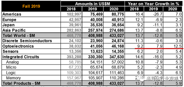 Data source: WSTS December 2019 Update
There are many professional investment institutions with rich experience in the field of integrated circuits and related industries in China. However, due to the late start of optical chips in China, it has only started to return to China to establish optical chip companies with a group of outstanding returnees in the past five years. For investment in optical chips, everyone basically refers to the experience of integrated circuit investment, and explores forward.
The exploration of DeLin Capital in the field of optical chips is actually accompanied by the growth of these excellent startup companies. At present, the three optical chips we have invested are: lemon photons at the laser emitting end (main products VCSEL, EEL, HCSEL), polar engraved photon at the photoelectric modulation end (high-speed electro-optic modulation chip based on lithium niobate film), and photodetector end Flying Core Optoelectronics (Lidar detection chip for car and mobile phone).
Combining the experience of these years, we feel that there is still a very significant difference between the investment of optical chips and the investment of integrated circuits. Here are some rough analysis for everyone to discuss and exchange.
High dependence on process and non-standardization of upstream foundry
The high dependence of the optical chip on the process and the non-standardization of upstream foundry are the biggest differences from the design of integrated circuits. Usually we will pay attention to chip design, manufacturing, market, etc. Integrated circuit investment usually starts from the market side, analyzes the market space, customer attributes, competition pattern, industry law, etc. of the subdivision track, and pays attention to the design part, including the team ’s Background, product definition, technical reserves, and mass production verification, etc. At these points, the investment logic of optical chips and integrated circuits is consistent.
The difference lies in the non-standardization of the upstream foundry of optical chips. Although there are epitaxial manufacturers such as IQE, Lianya, and New in the market, as well as OEM suppliers such as Wenmao and Hongjie, due to the diverse and complex structure of the optical chip itself, the manufacturing process has many know-hows and The requirements and focus of the process are also different, resulting in huge differences in the manufacturing modes of various products. For start-up companies, whether to choose outsourcing, joint development or self-built production lines, the path is different and the difference is significant.
For example, the multi-layer epitaxial structure of VCSEL makes its epitaxial requirements very high, but the lithography link is relatively standardized; the number of EEL chip layers is small, and the performance is reflected in the lithography link, the etching of the grating, and the coating on the end face. The application of EEL to optical communication or high power is different. DFB for communication requires extremely narrow wavelengths or wavelength stability. Therefore, the holographic, EBL or nano-imprint links used for manufacturing gratings are very important. The EEL used for power pump source has a key process secret in the cavity surface coating. For silicon light (including some modified silicon substrates), or manufacturing optical waveguides on some new materials (such as lithium niobate films), some special process exploration is needed. The non-standardization of these processes actually poses a huge challenge to the investment of early-stage optical chip companies. Investors need to understand the key technical thresholds and market competition from product design to manufacturing based on technical principles, chip structure and process flow Advantage.
When the startup company develops the corresponding strategy in the early stage, it needs to consider whether to choose the Fabless mode, the IDM mode, or the mode between the two (partial link OEM + partial link self-built production line). There are many options for which links must be built by themselves, which links can use standardized foundry, and which links are more suitable for joint development with upstream foundries. The startups have great challenges in terms of capital adequacy, market uncertainty, recruitment of craftsmen, and the recognition of the stability of the self-built production line and the process climbing by downstream major customers. For the founders, these challenges require sufficient experience and a high enough perspective; for investors, they also put forward extremely high requirements. Investors need to fully analyze the design structure and working principle of the chip, combined with the analysis of product application scenarios, customer pain points, and competitive landscape, to find opportunities for startups and determine whether the team has sufficient industry experience. And whether the strategic steps proposed by the team are really reasonable under the premise that the various conditions are relatively limited.
There are also a small number of entrepreneurial teams in the market who deliberately plan some production line equipment layouts to cater to investors. For example, some investors believe that optical chip companies must build MOCVD epitaxial links, which are more reliable than non-building. Once they hear epitaxy, lithography outside OEM, and optical packaging, they feel that the technical content may not be high. Such simple judgments are debatable.
Therefore, the investment of optical chips must be analyzed from the working principle, design points and process bottlenecks of the product, which has formed a huge difference from the model of integrated circuit standardization.
The market segmentation is limited, and horizontal expansion is obviously constrained by the technical span and process requirements
The application scenarios of several hot optical chips currently on the market include: sensing VCSEL and HCSEL for consumer electronics; VCSEL, DFB, EML, silicon photonics chip, lithium niobate thin film chip for communication; etc .; High power EEL, HCSEL for processing or pumping. For these subdivided fields, the market space for each application scenario is relatively limited, and it is difficult to find a market space as large as analog or memory chips in integrated circuits.
The design and manufacture of these chips have extremely high thresholds, and there are great challenges in crossing each other. There are many design and process differences between high-power EEL chips, sensor optical chips, and communication optical chips, and their respective process difficulties are different. The core technical personnel and key equipment required are also very different. Even for VCSEL, communication and sensing are also different technical challenges. Some of these optical chips focus on epitaxy, some focus on lithography, some focus on grating preparation, and some even focus on film packaging, etc. For most startups, it is difficult to expand laterally in multiple directions in the short to medium term . Unless the founding team itself has a lot of experience accumulated in foreign leading companies in these fields, such as Lemon Photon, the two founders have direct industries in the fields of high-power EEL, sensing VCSEL and the new generation of HCSEL experience. It should be emphasized that this industry experience must be the first-line mass production experience including design and process.
Looking at the world, the companies that currently make optical chips have not yet had a giant like integrated circuits, and the leading company Lumentum's revenue in fiscal 2019 is only about 1.5 billion US dollars. For start-up companies, it is extremely difficult to cross the three major fields of high power, communication, and sensing like Lumentum. Of course, Lumentum is also gradually acquired through mergers and acquisitions in the long-term development process. This is also the embarrassment of the investment in optical chips. The technical threshold is extremely high, and the single market space is relatively limited. The current VCSEL sensor can see the amount, which is only in the field of mobile phone 3D recognition and face payment. Radar, in-car gesture recognition and other directions are yet to be promoted. High-power EEL is mainly used as a pump source for fiber lasers. The application of direct semiconductor lasers in laser cladding and other fields is gradually being promoted. Communication is a big market. With the construction of 5G infrastructure and data centers, there will be certain opportunities for the localization of communication VCSEL, DFB and EML. Silicon optical chips and lithium niobate thin film modulation chips for emerging materials will also be gradually applied in the market.
In general, the application potential of optical chips is huge, and the high technical threshold makes horizontal expansion very difficult, making teams with practical experience and mass production capabilities in many aspects of the product line on the market very scarce. This is different from the field of integrated circuits. on the one hand.
Reliability challenges are higher than integrated circuits, and reliability bottlenecks are strongly related to chip structure
From the application side, optical chips and integrated circuits have reliability requirements, and the requirements are different in different application scenarios. From the product side, the reliability problem of the optical chip is more prominent than the integrated circuit: on the one hand, the high-power EEL chip, because of the long-term high-power emission concentrated on the output end surface, the end surface damage phenomenon is very significant, can it be alleviated This end-face damage effect has become the most important symbol for evaluating the company's research and development and production capacity of such products, which is also the core process secret of companies such as Lumentum.
Even on non-high-power optical chips for sensing or communication, due to the difference in material system (various doped GaAs, InP), and the complicated special structural design during the epitaxy process, the optical chip will be used over time. The extension and the impact of the use environment have deteriorated to varying degrees in performance. This is quite different from the mature silicon-based process of integrated circuits.
How to improve the reliability of optical chips is a great challenge for start-up companies. This challenge not only comes from design and process, but also from repeated verification, continuous improvement and rapid iteration of large downstream customers. This is also a paradox for startups. It is difficult for downstream large customers to accept a startup to replace core optical chips in some application scenarios with high reliability requirements, such as long-distance communication and high-power pumping. Sources, including mobile phone sensing, can have one or two sample delivery test opportunities are already commendable. Several reliability problems and failures will make downstream major customers directly lose confidence in startups. How to make the downstream major customers try their best to help the company try and verify the chip, iterate iteratively, improve reliability and stability, becomes a vital resource for product polishing and finally to the market. We tend to start-up companies with direct downstream strategic customer involvement. Only with this deep binding will we have the opportunity to obtain multiple application verifications at the early stage of the product, thereby rapidly improving reliability.
In summary, in the past two years and the foreseeable next few years, optical chips are the fastest growing semiconductor field that is in urgent need of localized replacement. However, the investment of optical chips is still very challenging for investment institutions. It needs to have sufficient professional knowledge and industry experience to comprehensively judge the feasibility of product design and process, the rationality of factory construction and OEM strategy, etc. We are more optimistic about a team that has first-line mass production experience in relatively many product lines, reliable verification that can be fully supported by large downstream customers, and has accumulated on the next generation of innovative product routes. I believe that such excellent optical chip startups can become bigger and stronger under the general trend of localization substitution, and on this basis, participate in global competition as soon as possible, and even lead the new direction of next-generation laser applications. .
Data source: WSTS December 2019 Update
There are many professional investment institutions with rich experience in the field of integrated circuits and related industries in China. However, due to the late start of optical chips in China, it has only started to return to China to establish optical chip companies with a group of outstanding returnees in the past five years. For investment in optical chips, everyone basically refers to the experience of integrated circuit investment, and explores forward.
The exploration of DeLin Capital in the field of optical chips is actually accompanied by the growth of these excellent startup companies. At present, the three optical chips we have invested are: lemon photons at the laser emitting end (main products VCSEL, EEL, HCSEL), polar engraved photon at the photoelectric modulation end (high-speed electro-optic modulation chip based on lithium niobate film), and photodetector end Flying Core Optoelectronics (Lidar detection chip for car and mobile phone).
Combining the experience of these years, we feel that there is still a very significant difference between the investment of optical chips and the investment of integrated circuits. Here are some rough analysis for everyone to discuss and exchange.
High dependence on process and non-standardization of upstream foundry
The high dependence of the optical chip on the process and the non-standardization of upstream foundry are the biggest differences from the design of integrated circuits. Usually we will pay attention to chip design, manufacturing, market, etc. Integrated circuit investment usually starts from the market side, analyzes the market space, customer attributes, competition pattern, industry law, etc. of the subdivision track, and pays attention to the design part, including the team ’s Background, product definition, technical reserves, and mass production verification, etc. At these points, the investment logic of optical chips and integrated circuits is consistent.
The difference lies in the non-standardization of the upstream foundry of optical chips. Although there are epitaxial manufacturers such as IQE, Lianya, and New in the market, as well as OEM suppliers such as Wenmao and Hongjie, due to the diverse and complex structure of the optical chip itself, the manufacturing process has many know-hows and The requirements and focus of the process are also different, resulting in huge differences in the manufacturing modes of various products. For start-up companies, whether to choose outsourcing, joint development or self-built production lines, the path is different and the difference is significant.
For example, the multi-layer epitaxial structure of VCSEL makes its epitaxial requirements very high, but the lithography link is relatively standardized; the number of EEL chip layers is small, and the performance is reflected in the lithography link, the etching of the grating, and the coating on the end face. The application of EEL to optical communication or high power is different. DFB for communication requires extremely narrow wavelengths or wavelength stability. Therefore, the holographic, EBL or nano-imprint links used for manufacturing gratings are very important. The EEL used for power pump source has a key process secret in the cavity surface coating. For silicon light (including some modified silicon substrates), or manufacturing optical waveguides on some new materials (such as lithium niobate films), some special process exploration is needed. The non-standardization of these processes actually poses a huge challenge to the investment of early-stage optical chip companies. Investors need to understand the key technical thresholds and market competition from product design to manufacturing based on technical principles, chip structure and process flow Advantage.
When the startup company develops the corresponding strategy in the early stage, it needs to consider whether to choose the Fabless mode, the IDM mode, or the mode between the two (partial link OEM + partial link self-built production line). There are many options for which links must be built by themselves, which links can use standardized foundry, and which links are more suitable for joint development with upstream foundries. The startups have great challenges in terms of capital adequacy, market uncertainty, recruitment of craftsmen, and the recognition of the stability of the self-built production line and the process climbing by downstream major customers. For the founders, these challenges require sufficient experience and a high enough perspective; for investors, they also put forward extremely high requirements. Investors need to fully analyze the design structure and working principle of the chip, combined with the analysis of product application scenarios, customer pain points, and competitive landscape, to find opportunities for startups and determine whether the team has sufficient industry experience. And whether the strategic steps proposed by the team are really reasonable under the premise that the various conditions are relatively limited.
There are also a small number of entrepreneurial teams in the market who deliberately plan some production line equipment layouts to cater to investors. For example, some investors believe that optical chip companies must build MOCVD epitaxial links, which are more reliable than non-building. Once they hear epitaxy, lithography outside OEM, and optical packaging, they feel that the technical content may not be high. Such simple judgments are debatable.
Therefore, the investment of optical chips must be analyzed from the working principle, design points and process bottlenecks of the product, which has formed a huge difference from the model of integrated circuit standardization.
The market segmentation is limited, and horizontal expansion is obviously constrained by the technical span and process requirements
The application scenarios of several hot optical chips currently on the market include: sensing VCSEL and HCSEL for consumer electronics; VCSEL, DFB, EML, silicon photonics chip, lithium niobate thin film chip for communication; etc .; High power EEL, HCSEL for processing or pumping. For these subdivided fields, the market space for each application scenario is relatively limited, and it is difficult to find a market space as large as analog or memory chips in integrated circuits.
The design and manufacture of these chips have extremely high thresholds, and there are great challenges in crossing each other. There are many design and process differences between high-power EEL chips, sensor optical chips, and communication optical chips, and their respective process difficulties are different. The core technical personnel and key equipment required are also very different. Even for VCSEL, communication and sensing are also different technical challenges. Some of these optical chips focus on epitaxy, some focus on lithography, some focus on grating preparation, and some even focus on film packaging, etc. For most startups, it is difficult to expand laterally in multiple directions in the short to medium term . Unless the founding team itself has a lot of experience accumulated in foreign leading companies in these fields, such as Lemon Photon, the two founders have direct industries in the fields of high-power EEL, sensing VCSEL and the new generation of HCSEL experience. It should be emphasized that this industry experience must be the first-line mass production experience including design and process.
Looking at the world, the companies that currently make optical chips have not yet had a giant like integrated circuits, and the leading company Lumentum's revenue in fiscal 2019 is only about 1.5 billion US dollars. For start-up companies, it is extremely difficult to cross the three major fields of high power, communication, and sensing like Lumentum. Of course, Lumentum is also gradually acquired through mergers and acquisitions in the long-term development process. This is also the embarrassment of the investment in optical chips. The technical threshold is extremely high, and the single market space is relatively limited. The current VCSEL sensor can see the amount, which is only in the field of mobile phone 3D recognition and face payment. Radar, in-car gesture recognition and other directions are yet to be promoted. High-power EEL is mainly used as a pump source for fiber lasers. The application of direct semiconductor lasers in laser cladding and other fields is gradually being promoted. Communication is a big market. With the construction of 5G infrastructure and data centers, there will be certain opportunities for the localization of communication VCSEL, DFB and EML. Silicon optical chips and lithium niobate thin film modulation chips for emerging materials will also be gradually applied in the market.
In general, the application potential of optical chips is huge, and the high technical threshold makes horizontal expansion very difficult, making teams with practical experience and mass production capabilities in many aspects of the product line on the market very scarce. This is different from the field of integrated circuits. on the one hand.
Reliability challenges are higher than integrated circuits, and reliability bottlenecks are strongly related to chip structure
From the application side, optical chips and integrated circuits have reliability requirements, and the requirements are different in different application scenarios. From the product side, the reliability problem of the optical chip is more prominent than the integrated circuit: on the one hand, the high-power EEL chip, because of the long-term high-power emission concentrated on the output end surface, the end surface damage phenomenon is very significant, can it be alleviated This end-face damage effect has become the most important symbol for evaluating the company's research and development and production capacity of such products, which is also the core process secret of companies such as Lumentum.
Even on non-high-power optical chips for sensing or communication, due to the difference in material system (various doped GaAs, InP), and the complicated special structural design during the epitaxy process, the optical chip will be used over time. The extension and the impact of the use environment have deteriorated to varying degrees in performance. This is quite different from the mature silicon-based process of integrated circuits.
How to improve the reliability of optical chips is a great challenge for start-up companies. This challenge not only comes from design and process, but also from repeated verification, continuous improvement and rapid iteration of large downstream customers. This is also a paradox for startups. It is difficult for downstream large customers to accept a startup to replace core optical chips in some application scenarios with high reliability requirements, such as long-distance communication and high-power pumping. Sources, including mobile phone sensing, can have one or two sample delivery test opportunities are already commendable. Several reliability problems and failures will make downstream major customers directly lose confidence in startups. How to make the downstream major customers try their best to help the company try and verify the chip, iterate iteratively, improve reliability and stability, becomes a vital resource for product polishing and finally to the market. We tend to start-up companies with direct downstream strategic customer involvement. Only with this deep binding will we have the opportunity to obtain multiple application verifications at the early stage of the product, thereby rapidly improving reliability.
In summary, in the past two years and the foreseeable next few years, optical chips are the fastest growing semiconductor field that is in urgent need of localized replacement. However, the investment of optical chips is still very challenging for investment institutions. It needs to have sufficient professional knowledge and industry experience to comprehensively judge the feasibility of product design and process, the rationality of factory construction and OEM strategy, etc. We are more optimistic about a team that has first-line mass production experience in relatively many product lines, reliable verification that can be fully supported by large downstream customers, and has accumulated on the next generation of innovative product routes. I believe that such excellent optical chip startups can become bigger and stronger under the general trend of localization substitution, and on this basis, participate in global competition as soon as possible, and even lead the new direction of next-generation laser applications. .