


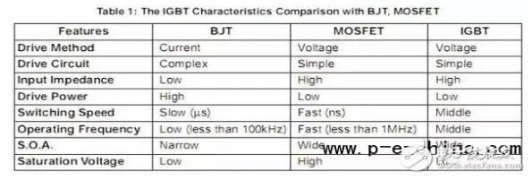
The IGBT is a voltage-controlled power transistor that you can think of as a high-power version of the CMOS tube. Features are high switching frequency, the main application of the family, such as inverter air conditioners, induction cookers, microwave ovens, there is the active power supply of the computer power supply and UPS. Industrial applications are mainly used for various motor drives. From a functional point of view, IGBTs are circuit switches that are used in tens to hundreds of volts and currents of tens to hundreds of amperes.
When we talk about IGBTs, people in semiconductor manufacturing think that it is not a discrete device (Power Disceret). However, like 28nm/16nm integrated circuit manufacturing, he is a key supporting project of the “02 Special Project” of the country. This gadget is the most technologically advanced product in power electronics, and has completely replaced the traditional Power mosFET, and its application is very extensive. , small appliances, large strategic industry to aircraft, ships, transportation, power grids and other power electronics industry is known as the "CPU", a long time, the product (including chips) is still a monopoly in the hands of a small number of IDM ( Fairchild, Infineon, and TOSHIBA are among the country's 16 major technological breakthroughs during the 12th Five-Year Plan period (abbreviated as “02 Special”).
1. What is an IGBT?
The IGBT is called Insulated Gate Bipolar Transistor, so it is a BJT transistor with MOS Gate. Strange, is it a MOSFET or a BJT? In fact, they are not both. Without a circle, he is a combination of MOSFET and BJT.
The main MOSFET single carriers (sub-multiple) conductive while both carriers BJT is electrically conductive, so that the driving current of the BJT will be larger than the MOSFET, but the stage control gate of the MOSFET is a field effect by controlled inversion, There is no additional control power loss. Therefore, IGBT is a combination of the advantages of MOSFET and BJT. It also has a MOSFET gate voltage control transistor (high input impedance) and uses BJT's dual carrier to achieve high current (low turn-on voltage drop). (Voltage-Controlled Bipolar Device). So as to achieve a small drive power, saturation pressure reduction of the perfect requirements, widely used in more than 600V converter systems such as AC motors, inverters, switching power supply, lighting circuits, traction drives and other fields.
2.the traditional power MOSFET
In order to wait for the convenience of understanding the IGBT, I will first talk about the structure of the Power MOSFET. The so-called power MOS is to withstand high power, in other words, high voltage, high current. We combine the general low voltage MOSFET to explain how to change the structure to achieve high voltage and high current.
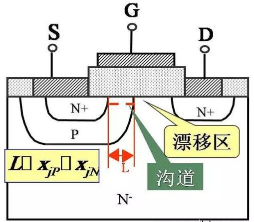
1) High voltage: General MOSFET If Drain's high voltage, it is easy to cause device breakdown, and the general breakdown channel is the other three terminals of the device (S/G/B), so to solve the high voltage problem must be blocked end. The Gate can only rely on the Field-Plate of the field oxygen pad under the gate, while the PN junction breakdown at the Bulk end can only rely on reducing the concentration of the two sides of the PN junction, and the most annoying is to the Source end. A long drift region is needed as a series resistor divider for the drain, allowing the voltage to drop in the drift region.
2) High current: The channel length of a common MOSFET is determined by Poly CD, and the channel of a power MOSFET is controlled by the junction depth of two diffusions. Therefore, as long as the process is stable, it can be done very small and not affected by light. Accuracy limits. The current of the device depends on W/L, so if you want to get a large current, you only need to increase W.
So the above Power MOSFET is also called LDMOS (Lateral Double diffusion MOS). Although such a device can achieve high power requirements, it still has its inherent disadvantages. Since its source, gate, and drain terminals are all on the surface, the drain and source electrodes need to be pulled long, which wastes the chip area. Moreover, because the device is on the surface, if the device and the device are to be connected in parallel, the complexity increases and isolation is needed. So VDMOS (VerTIcal DMOS) was later developed, and the drains were put on the back of the Wafer, so that the length of the drift region of the drain and the source can be completely controlled by the backside thinning, and this structure is more conducive to the pipe between The parallel structure achieves high power. However, the LDMOS structure is still used in the BCD process to be compatible with CMOS.
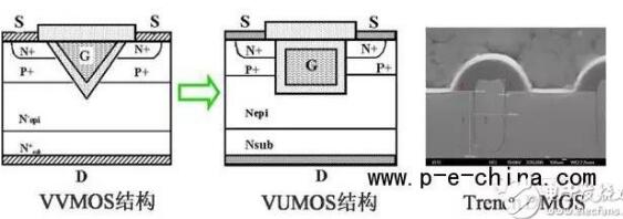
Let us talk about the development and evolution of VDMOS. The earliest VDMOS is to directly put the Drain of LDMOS on the back through thinning of the back face, Implant, and metal evaporation (as shown below). He is the legendary Planar VDMOS. The challenge with traditional LDMOS lies in the backside process. But its advantage is that the positive process is compatible with the traditional CMOS process, so it is still alive. However, the disadvantage of this structure is that the channel is horizontal and the area utilization is still not high enough.
Later, in order to overcome the shortcomings of Planar DMOS, VMOS and UMOS structures were developed. Their approach was to dig a groove in the surface of Wafer, turning the channel of the tube from the original Planar into a verTIcal along the wall of the tank, which was really a clever idea. However, a pie is always associated with a trap (IC manufacturing is always in a trade-off), and the inherent disadvantage of this structure is that the slot is too deep and it is easy for the electric field to concentrate and cause breakdown, and the process is difficult and costly, and The bottom of the groove must be absolutely rouding, otherwise it will break down easily or produce stress lattice defects. But its advantage is that the number of crystals is much more than the original, so more transistors can be connected in parallel, which is more suitable for low voltage and high current applicaTIon.
There is also a classic thing called CoolMOS, everyone google learning it. He should be regarded as the highest voltage of Power MOS, can reach 1000V.
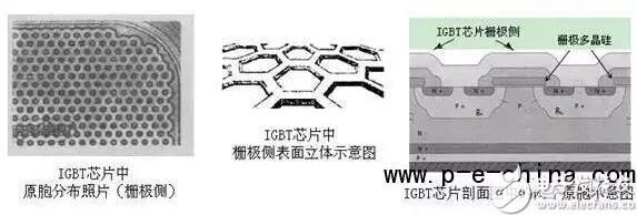
3.IGBT structure and principle
The above describes the Power MOSFET, and the IGBT is essentially a field effect transistor. From the structural point of view, it is very close to the Power MOSFET. A P+ layer is added to the drain electrode on the back. We call it InjecTIon Layer (the origin of the name, etc.) Said below). . The Power MOSFET described above is essentially a traditional MOSFET. It is still a single carrier (multiple) conduction, so we have not yet played its ultimate performance. So, afterwards, we developed a new structure. How can we be able to inject holes from the drain side of the MOSFET's own electrons when the Power MOSFET is turned on? So it is natural to introduce a P+ injection layer (which is the origin of the name) at the drain end, and a P+/N-drift PN junction is added to the drain structure. However, it is a positive bias, so it is not The effect of conduction is to increase the hole injection effect, so its characteristics are similar to BJT. There are two kinds of carriers involved in conduction. So the original source becomes Emitter, and Drain becomes Collector.
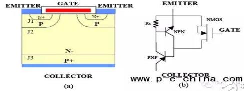
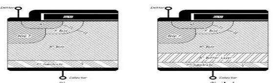
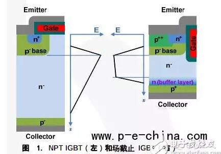
This structural advantage is to improve the current drive capability, but the downside is that when the device is turned off, the channel is quickly turned off without multi-sub-current, but the Collector (Drain) side continues to have a minority injection hole, so the entire The current of the device needs to be slowly turned off (tailing current), which affects the turn-off time and operating frequency of the device. This is a taboo for switching devices, so it has introduced a structure to add an N+buffer layer between P+ and N-drift. The role of this layer is to allow holes to be injected from the Collector when the device is powered off. The N+ buffer layer is rapidly compounded to increase the turn-off frequency. We call this structure a PT-IGBT (Punch Through type), whereas an NPT-IGBT was originally used without an N+ buffer.
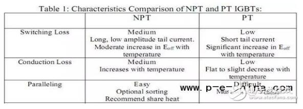
In general, NPT-IGBT is higher than Vce(sat) of PT-IGBT, mainly because NPT is positive temperature coefficient (P+ substrate has less hole injection), and PT is negative temperature coefficient (since P substrate is thicker. Therefore, the triode base modulation effect caused by the more hole injection is obvious), and Vce(sat) determines the switch loss, so if the same Vce(sat) is needed, the NPT must increase the drift thickness. Ron has grown.
4.IGBT manufacturing process:
The front of the IGBT module process and the standard BCD LDMOS is not bad, but the back is more difficult:
1) Back thinning: General requirements are 6~8mil, this thickness is hard to grind, and it is easy to fragment.
2) Back-injection: Grind 6 to 8 mils, and hit the high current P+ implant ”E14's dose. It's easy to shard. There must be a dedicated device dedicate. Even the fourth generation has two Hi-current injections, which is even more challenging.
3) Backside cleaning: This general SEZ is fine.
4) Backside metallization: This can only be done with metal evaporation process, Ti/Ni/Ag standard process.
5) The back of Alloy: The main consideration is that wafer is too thin and it is easy to warp debris.
5, IGBT's new technology:
1) Field cut-off FS-IGBT: No matter whether PT or NPT structure can not meet the requirement of infinite high power, in order to achieve high power, it is necessary to reduce Vce(sat), that is, reduce Ron. Therefore, the N-drift thickness must be reduced, but the N-drift thickness is again constrained by the off-state electric field (too thin for easy channel punch-through). Therefore, if you want to reduce the drift thickness, you must let the cut-off electric field fall ahead of the channel. Therefore, it is necessary to introduce an N+ field stop (FS) between the P+ injection layer and the N-drift. When the IGBT is turned off, the electric field is rapidly reduced to 0 in the cutoff layer to achieve the purpose of termination, so we can Further reduce the N-drift thickness to reduce Ron and Vce. And this structure is very similar to the N+ buffer structure, so it also has the effect of the PT-IGBT to suppress the tailing current in the off state to increase the off speed.
The question is, what is the difference between this and the PT-IGBT's N+ buffer? In fact, the production process is not the same. The PT-IGBT is made of two layers of EPI. It is the first layer of ~10um of N+ buffer on the P+ substrate, and the second layer of ~100um of N-Drift. This cost is very high! In contrast, FS-IGBTs are based on NPT-IGBTs, which directly penetrate the high-concentration N+ cut-off layer directly on the back side. The cost is relatively low, but the challenge is how to achieve no-fragmentation at thinner thicknesses.
2) Anode shorted (SA: Shorted-Anode): Its structure is that the N+ collector is intermittently inserted into the P+ collector so that the N+ collector directly contacts the field stop layer and acts as a cathode of the PN diode, and P+ continues to do its FS - The collector of the IGBT, which has enhanced current characteristics and changes the cost structure because no co-packaged anti-parallel diodes are needed. Experiments have shown that it can increase the saturation current and reduce the saturation pressure drop (~12%).
6. Main I-V characteristics of IGBT:
You can use it as a MOSFET in series with a PiN diode, or as a wide base PNP driven by a MOSFET (DarlinGTOn structure). The former can be used to understand its characteristics, and the latter is his principle. It looks like the IV curve of a MOSFET is shifted backwards ("0.7V) because the channel-opening current must satisfy the product of the drift region current and the drift resistance over 0.7V to make the P+ substrate and N-drift The PN junction is conducting so that it can work. Otherwise, the channel cannot be opened.
We often hear the first generation of IGBTs up to the sixth generation of IGBTs. What do these mean?
1) The first generation: He is the prototype of IGBT, the simplest kind of schematic structure, so he must increase N-drift to improve the withstand voltage, so on-resistance and turn-off power consumption are relatively high, so there is no universal use.
2) The second generation: PT-IGBTs, because the depletion layer cannot penetrate the N+ buffer layer, the electric field strengthening of the base area is trapezoidal, so the chip thickness can be reduced and the power consumption can be reduced. This is mainly the Siemens product BSM150GB120DN1 from 1990 to 1995 ("DN1" means the first generation). It has an advantage mainly at 600V (similar to GTR characteristics), and when it comes to 1200V, it encounters the problem that the epitaxial thickness is large, the cost is high, and the reliability is low (the uniformity of doping concentration and thickness is poor).
3) The third generation: NPT-IGBT, which no longer uses epitaxial technology, uses ion implantation technology to generate P+ collector (transparent collector technology), which can accurately control the junction depth and control the emission efficiency as low as possible. Fast carrier extraction speed to reduce turn-off loss, can maintain the original carrier life of the base area without affecting the steady-state power consumption, and has a positive temperature coefficient characteristic, so the technology is more mature in the steady-state loss and turn-off The loss has made a good compromise, so it is widely used. On behalf of the company is still Siemens took the lead in adopting FZ (zone melting method) instead of epitaxial bulk products, on behalf of the product BSM200GB120DN2, VCE "1200V, Vce (sat) = 2.1V.
4) The fourth generation: Trench-IGBT, the biggest improvement is the use of Trench structure, the channel is running from the surface to the vertical surface, so the PIN effect of the base area is enhanced, the concentration of carriers near the gate increases, thereby increasing The conductance modulation effect reduces the on-resistance, and since the channel is not on the surface, the JFET effect is eliminated, so the gate density increase is not limited, and the third-generation collector P+ continues to be used in the fourth-generation IGBT. The implant technology also incorporates the second-generation PT technology as a field stop layer, which is particularly effective for high pressure resistance. Need to use dual injection technology, it is more difficult. This time is the era of Infineon, Infineon thinning technology in the world, its thickness can be reduced to 120um ~ 140um at 1200V (NPT-IGBT needs 200um), even at 600V can be reduced to 70um.
5) The fifth generation: FS-IGBT and the sixth generation FS-Trench. The fifth and sixth generation products are the recombination of various technical measures after the IGBT has undergone the above four technical improvement practices. The fifth-generation IGBT is a combination of the fourth-generation product "transparent collector area technology" and "electric field suspension technology." The sixth generation of products is based on the fifth generation of improved trench gate structure, and a new look.
At present, China's overall energy efficiency is about 33%, which is about 10% lower than that of developed countries. At present, China's energy-saving work is under great pressure. In the field of new energy, China has become the largest country in the production of solar cells. The cumulative installed capacity of wind power has also been doubled for four years in a row, which means that China's new energy market has huge business opportunities. Whether it is solar cells, wind power or new energy vehicles, their system applications need to convert direct current into alternating current. The component that undertakes this task is called an inverter. The core device of the inverter is IGBT (Insulated Gate Bipolar Transistor), which is also one of the most expensive components. In foreign countries, IGBT technology and products are continuously updated, and China currently does not have the ability to mass produce IGBTs. All of them are IGBT technology for high-speed railways produced by Zhuhai Hainan Vehicle and CNR, as well as China Resources Microelectronics (who wants to acquire Fairchild), and Huahong Hongli seem to have it. Now the country mainly supports 8-inch IGBT technology.