


IGBT, insulated gate bipolar transistor (Insulated Gate Bipolar Transistor), which is by the BJT (bipolar transistor) and MOS (insulated gate type field effect transistor) composed of composite full control voltage-driven power semiconductor devices.
IGBT is a high-power power electronic devices, is a non-pass that is off the switch, IGBT does not amplify the voltage function, conduction can be seen as a wire, open as open circuit. The three major features are high pressure, high current, high speed. It is a very effective tube in the field of power electronics.
BJT (Bipolar Junction Transistor): Bipolar transistor, "bipolar" means that there are two kinds of carriers with different polarity charge to participate in conduction.
FET: A semiconductor device that controls the output loop current by controlling the electric field effect of the input circuit. It is dominated by only the majority of carriers in the semiconductor, also known as unipolar transistors.
IGBT development history comparison:
|
Product |
Features |
|
SCR |
Power capacity, the current level has reached 7000V / 8000A. But the disadvantage is the low switching speed, turn off uncontrollable, forced commutation off the control circuit is very complex, limiting its application. |
|
GTO、GTR |
They are self-shut-off devices, switching speed than SCR high, the control circuit has also been simplified. The current GTO and GTR levels are 6000V and 6000A, 1000V and 400A, respectively. But the GTO switching speed is still relatively low, GTR there is a second breakdown and difficult to parallel problems. In addition, they co-exist the drive current, loss of power consumption problems. |
|
VDMOS、SIT |
High switching speed, high input impedance, low control power, simple driving circuit and so on. But the conductivity limits their current capacity and power capacity. However, the use of ultra-large-scale IC technology to VDMOS cell size is very small (only a few square microns), greatly increasing the number of cells, reducing the on-resistance, improve the current capacity. However, the power capacity is still very low. 100V or less, VDMOS is the ideal switching device. |
|
IGBT |
At present, IGBT devices from the first generation to the fourth generation, its operating frequency can reach 200KHz. Its power capacity from small power (80-300A / 500-1200V) single tube to the development of ultra-high power (1000-1200A / 2500-4500V) module, forming a series of products, product coverage is very large. |
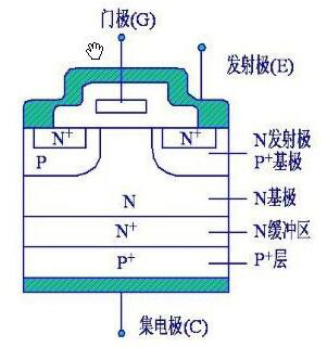
The figure above shows an N-channel enhancement type insulated gate bipolar transistor structure, the N + region is called the source region, and the electrode attached to it is called the source (ie, emitter E). N base is called drain. The control area of the device is a gate region, and the electrode attached to it is called a gate (gate G). The channel is formed close to the boundary of the gate. The P-type (including the P + and P-regions) (the channel is formed in this region) between the C and E poles is called the subchannel region. The P + region on the other side of the drain region is called the Drain injector, which is a specific functional region of the IGBT. Together with the drain and subchannel regions, the PNP bipolar transistor acts as an emitter. Drain the hole into the conductive modulation to reduce the device's on-state voltage. The electrode attached to the drain injection region is called a drain (i.e., collector C).
IGBT switch function is by adding a positive gate voltage to form a channel, to the PNP (originally NPN) transistor to provide the base current, the IGBT conduction. Instead, add a reverse gate voltage to eliminate the channel, cut off the base current, and turn the IGBT off. IGBT drive method and MOSFET are basically the same, just control the input N-channel MOSFET, so with high input impedance characteristics. When the channel of the MOSFET is formed, the N-layer is inductively modulated from the P + base to the hole of the N-layer, and the resistance of the N-layer is reduced, so that the IGBT has a low voltage Of the on-state voltage.
How IGBT works
method
IGBT is a natural evolution of vertical power MOSFETs for high current, high voltage applications and fast terminal equipment. Since the realization of a higher breakdown voltage BVDSS requires a source and drain channel, and this channel has a high resistivity, resulting in the power MOSFET has a high RDS (on) high value, IGBT eliminates the existing power MOSFET Major shortcomings. Although the latest generation of power MOSFET devices significantly improve the RDS (on) feature, but at high levels, the power conduction loss is still much higher than the IGBT technology. The lower voltage drop, the ability to convert to a low VCE (sat), and the IGBT's structure, compared to a standard bipolar device can support higher current densities and simplify the schematic of the IGBT driver.
The structure of the IGBT wafers is very similar to that of the power MOSFETs. The main difference is that the IGBT module adds the P + substrate and an N + buffer layer (NPT-non-pass-IIGTT technology does not add this part). As shown in the equivalent circuit diagram, one of the MOSFETs drives two bipolar devices. The application of the substrate creates a J1 junction between the P + and N + regions of the tube. When the positive gate bias causes the bottom of the gate to invert the P base region, an N-channel is formed while an electron flow occurs and a current is generated exactly as the power MOSFET. If the voltage generated by this electron current is in the range of 0.7V, then J1 will be in the forward bias, some holes injected into the N-zone, and adjust the resistivity between the anode and cathode, this way reduces the power conduction The total loss and start the second charge flow. The final result is that there are two different current topologies in the semiconductor hierarchy: an electron current (MOSFET current); a hole current (bipolar).
When a negative bias or gate voltage is applied below the threshold, the channel is forbidden and no holes are injected into the N-zone. In any case, if the MOSFET current drops rapidly during the switching phase, the collector current is gradually reduced, because there is still a small number of carriers (minority) in the N layer after the commutation begins. The reduction of this residual current value (wake) depends entirely on the density of the charge at turn-off, and the density is related to several factors such as the number of dopants and the topological, thickness and temperature. The attenuation of the multiplier causes the collector current to have a characteristic wake waveform, and the collector current causes the following problems: power increases; cross-over problems, especially on devices using freewheeling diodes, are more noticeable.
In view of the fact that the wake is related to the recombination of the minority, the current value of the wake should be closely related to the hole mobility of the chip temperature, IC and VCE. Thus, depending on the temperature achieved, it is feasible to reduce the undesirable effect of this effect on the current design of the terminal device.
Block and latch
When the collector is applied a reverse voltage, J1 will be reverse bias control, depletion layer will be extended to the N-zone. This mechanism is important because it reduces the thickness of this level too much and will not be able to achieve an effective blocking capability. On the other hand, if the area size is too large, the pressure drop is continuously increased. The second point clearly illustrates the reason why the voltage drop of the NPT device is higher than that of the equivalent device (IC and speed).
IGBT has a parasitic PNPN thyristor between the collector and emitter. Under special conditions, this parasitic device will turn on. This phenomenon will increase the current between the collector and the emitter, reduce the control of the equivalent MOSFET, and usually cause device breakdown. Thyristor conduction phenomenon is called IGBT latch, in particular, the reasons for this defect are different, and the state of the device are closely related.