


Silicon is the most important base material for the integrated circuit industry. In today's information age, our daily use of mobile phones, computers, home appliances, cars and even large aircraft, are inseparable from the silicon after several processes made of semiconductor chips. At present, China is the world's largest semiconductor chip in the country, and independent production capacity is close to zero, the market is almost all monopoly by foreign companies.
By the silicon wafer "turned" for a variety of sizes of semiconductor components, which need a complex number of intermediate process steps, and Nanjing crystal can capture the most source of the industry chain "long crystal" process, they developed a For the "crystal growth" of the furnace, commonly known as "long crystal furnace." "The reason why good to do this, and we come to Nanjing at the beginning of the choice of sapphire Changjing market are inseparable." Nanjing crystal general manager Wu Chunsheng told reporters that their entrepreneurial team to returnees as early as 2012 aimed at sapphire Single crystal in the field of LED and smart phones are widely used in the market prospects in Nanjing Development Zone registered the establishment of the Nanjing Jing Sheng Energy Equipment Co., Ltd..
Nanjing Jing Sheng, chairman of Li Hui introduced their entrepreneurial team has a wealth of semiconductor single crystal furnace design and process development experience of the international top experts in the world of crystal materials in the field of the highest scientific research in New York, the United States set up overseas research and development center. Experts will be the most advanced thermal design and crystal growth control technology, transplanted into the sapphire crystal growth, the first in the country developed a 85 kg sapphire single crystal furnace, compared with similar foreign products, the price is low Nearly half.
Since then, in the 85 kilograms of long crystal furnace on the basis of Nanjing Jing Sheng has successfully made 120 kilograms of sapphire crystal furnace, has received seven patents, 16 utility model patents, in addition to more than 10 patents in the application The These are for this start-up time is not long high-tech enterprises to enter the semiconductor single crystal growth field laid the foundation.
Aimed at "large silicon made in China" special science and technology to start a new round of research and development
Why promote the localization of semiconductor chips? A data can explain the problem, the current annual purchase of imported chips to spend up to more than 2000 billion dollars, and even more than the amount of crude oil imports. Chip manufacturing is subject to people, not only will directly hinder the development of China's IC industry, information security is also a huge hidden dangers. At present, China's silicon wafer consumption is the world's first, of which 12-inch large silicon monthly demand will be more than 1 million, the domestic semiconductor business supply is almost zero. It is to attach importance to the weak link in this industry chain, "National Medium and Long-term Science and Technology Development Plan (2006-2020)" identified 16 major projects, "very large scale integrated circuit manufacturing equipment and complete sets of special" Out of it.
"In 2014, we heard from customers about the 'big silicon localization' project is about to start the news, focusing on manufacturing 40-28 nm 12-inch large silicon, immediately identified this as a new round of research and development direction "Li Hui said," After consultation with foreign experts team, we believe that sapphire crystal technology and semiconductor silicon long crystal furnace is the core technology platform is consistent, the experts use simulation software on the entire hot field involved, Silver Wing local air flow control , The internal magnetic field distribution and other factors affecting the crystal production to do a lot of computing and verification, after two years of research and development, and finally developed for 12 - inch semiconductor wafer manufacturing, cost - effective single crystal growth equipment.
The use of Nanjing crystal can develop the "long crystal furnace", one can produce a 1.5-meter-long thick silicon rod, cut into 1500 diameter 12 inches, 1 mm thick silicon, the downstream business can be directly used for semiconductor components Of the production, and 12-inch silicon is the current production of the brand mobile phones, computers and all kinds of storage equipment chip must be raw materials.
Beyond the import of equipment, "large silicon domestic project" manufacturing raw materials
Want to change the semiconductor chip completely dependent on the status of imports to solve the localization of silicon raw materials is the first step. Nanjing crystal in the country took the lead in developing a silicon wafer to help the production of the key equipment, but want the market to accept a start-up enterprises developed domestic equipment, began to be difficult.
"Our first customer is from Shanghai's new Sheng Semiconductor, they are currently the only commercial 12-inch semiconductor wafer manufacturers, commitment to the national science and technology special 28-nanometer 12-inch large silicon domestic projects in the second half of last year , The new Sheng procurement of three equipment, two from South Korea, one is made by us. "Li Hui introduced," the customer at the beginning or some skeptical, specifically to the United States saw our overseas R & D center, and ultimately agreed to give us a try A chance to try. "
Last year in September, Nanjing crystal developed the first 12-inch 350KG semiconductor monocrystalline silicon furnace delivered to customers for several months of stable operation, its advanced technology, the use of energy-saving and other indicators even beyond the foreign equipment, cost-effective. Soon, Nanjing Jingneng received the second order of the new Sheng, the new two equipment recently to be delivered. According to the new plan, the cumulative installed capacity of more than 60 units, and Nanjing Jing energy follow-up orders are still in negotiations.
"At present, we are working with customers to improve the silicon wafer technology, the future will continue through technological improvements and independent research and development, for the large silicon domestic projects to make greater contributions." Li said.
Want to change the chip depends on the status of imports, the raw material production must first step to achieve localization, to this end, the state launched the "big silicon domestic" major science and technology special. Nanjing Development Zone Xingzhi Technology Park, a start-up - Nanjing Jingneng Semiconductor Technology Co., Ltd. aimed at this opportunity, the first in China to develop a "12-inch semiconductor monocrystalline silicon furnace", and in the same competition with foreign equipment Win, as "large silicon localization" project in the production of silicon raw materials, the key equipment.
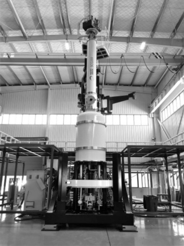
Made 12-inch 350KG semiconductor monocrystalline silicon furnace
By the silicon wafer "turned" for a variety of sizes of semiconductor components, which need a complex number of intermediate process steps, and Nanjing crystal can capture the most source of the industry chain "long crystal" process, they developed a For the "crystal growth" of the furnace, commonly known as "long crystal furnace." "The reason why good to do this, and we come to Nanjing at the beginning of the choice of sapphire Changjing market are inseparable." Nanjing crystal general manager Wu Chunsheng told reporters that their entrepreneurial team to returnees as early as 2012 aimed at sapphire Single crystal in the field of LED and smart phones are widely used in the market prospects in Nanjing Development Zone registered the establishment of the Nanjing Jing Sheng Energy Equipment Co., Ltd..
Nanjing Jing Sheng, chairman of Li Hui introduced their entrepreneurial team has a wealth of semiconductor single crystal furnace design and process development experience of the international top experts in the world of crystal materials in the field of the highest scientific research in New York, the United States set up overseas research and development center. Experts will be the most advanced thermal design and crystal growth control technology, transplanted into the sapphire crystal growth, the first in the country developed a 85 kg sapphire single crystal furnace, compared with similar foreign products, the price is low Nearly half.
Since then, in the 85 kilograms of long crystal furnace on the basis of Nanjing Jing Sheng has successfully made 120 kilograms of sapphire crystal furnace, has received seven patents, 16 utility model patents, in addition to more than 10 patents in the application The These are for this start-up time is not long high-tech enterprises to enter the semiconductor single crystal growth field laid the foundation.
Aimed at "large silicon made in China" special science and technology to start a new round of research and development
Why promote the localization of semiconductor chips? A data can explain the problem, the current annual purchase of imported chips to spend up to more than 2000 billion dollars, and even more than the amount of crude oil imports. Chip manufacturing is subject to people, not only will directly hinder the development of China's IC industry, information security is also a huge hidden dangers. At present, China's silicon wafer consumption is the world's first, of which 12-inch large silicon monthly demand will be more than 1 million, the domestic semiconductor business supply is almost zero. It is to attach importance to the weak link in this industry chain, "National Medium and Long-term Science and Technology Development Plan (2006-2020)" identified 16 major projects, "very large scale integrated circuit manufacturing equipment and complete sets of special" Out of it.
"In 2014, we heard from customers about the 'big silicon localization' project is about to start the news, focusing on manufacturing 40-28 nm 12-inch large silicon, immediately identified this as a new round of research and development direction "Li Hui said," After consultation with foreign experts team, we believe that sapphire crystal technology and semiconductor silicon long crystal furnace is the core technology platform is consistent, the experts use simulation software on the entire hot field involved, Silver Wing local air flow control , The internal magnetic field distribution and other factors affecting the crystal production to do a lot of computing and verification, after two years of research and development, and finally developed for 12 - inch semiconductor wafer manufacturing, cost - effective single crystal growth equipment.
The use of Nanjing crystal can develop the "long crystal furnace", one can produce a 1.5-meter-long thick silicon rod, cut into 1500 diameter 12 inches, 1 mm thick silicon, the downstream business can be directly used for semiconductor components Of the production, and 12-inch silicon is the current production of the brand mobile phones, computers and all kinds of storage equipment chip must be raw materials.
Beyond the import of equipment, "large silicon domestic project" manufacturing raw materials
Want to change the semiconductor chip completely dependent on the status of imports to solve the localization of silicon raw materials is the first step. Nanjing crystal in the country took the lead in developing a silicon wafer to help the production of the key equipment, but want the market to accept a start-up enterprises developed domestic equipment, began to be difficult.
"Our first customer is from Shanghai's new Sheng Semiconductor, they are currently the only commercial 12-inch semiconductor wafer manufacturers, commitment to the national science and technology special 28-nanometer 12-inch large silicon domestic projects in the second half of last year , The new Sheng procurement of three equipment, two from South Korea, one is made by us. "Li Hui introduced," the customer at the beginning or some skeptical, specifically to the United States saw our overseas R & D center, and ultimately agreed to give us a try A chance to try. "
Last year in September, Nanjing crystal developed the first 12-inch 350KG semiconductor monocrystalline silicon furnace delivered to customers for several months of stable operation, its advanced technology, the use of energy-saving and other indicators even beyond the foreign equipment, cost-effective. Soon, Nanjing Jingneng received the second order of the new Sheng, the new two equipment recently to be delivered. According to the new plan, the cumulative installed capacity of more than 60 units, and Nanjing Jing energy follow-up orders are still in negotiations.
"At present, we are working with customers to improve the silicon wafer technology, the future will continue through technological improvements and independent research and development, for the large silicon domestic projects to make greater contributions." Li said.