


Different internal structure of MOSFET and IGBT, determines the different areas of their applications.
1, due to the structure of the MOSFET, usually it can be done to a large current, you can go to KA, but the precondition voltage capability without IGBT strong.
2, IGBT can be very powerful, current and voltage can be, that is, the frequency is not too high, the current IGBT hard switching speed can be 100KHZ, it is already good. However, relative to the MOSFET's operating frequency is still a drop in the bucket, the MOSFET can work to hundreds of KHZ, MHZ, and even dozens of MHZ, RF products.

3, its application, according to its characteristics: MOSFET used in switching power supplies, ballasts, high frequency induction heating, high frequency inverter welding machine, communications power supply and so on high frequency power supply. IGBT focus on welding, inverters, inverters, electrolytic plating power supply, super audio induction heating and other fields.
The performance of the Switch Mode Power Supply (SMPS) is heavily dependent on the choice of power semiconductor devices, namely the switch and the rectifier.
Although there is no comprehensive solution to the problem of selecting IGBTs or MOSFETs, comparing the performance of IGBTs and MOSFETs in specific SMPS applications, it is still possible to determine the range of key parameters.
1, conduction loss
In addition to IGBT voltage drop longer, IGBT and power MOSFET conduction characteristics are very similar. It can be seen from the basic IGBT equivalent circuit (see Figure 1) that the time required to fully regulate minority carriers in the PNP BJT collector base region results in the occurrence of a voltage tailing voltage.
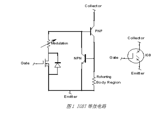
This delay causes a Quasi-saturation effect so that the collector / emitter voltage does not immediately drop to its VCE (sat) value. This effect also causes the VCE voltage to rise in the ZVS case at the moment when the load current is switched from the shunt-connected, antiparallel diode of the package to the collector of the IGBT.
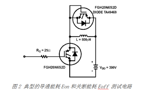
The Eon energy consumption listed in the IGBT datasheet is the time integral of the product of Icollector and VCE for each conversion cycle in Joules and contains additional losses related to class saturation. It is further divided into two Eon energy parameters, Eon1 and Eon2. Eon1 does not include the power loss associated with hard switching diode losses and Eon2 includes the hard switching turn-on energy associated with diode recovery, which can be measured by restoring the same diode as the diode-packaged diode. Typically, Eon2 test circuit shown in Figure 2. The IGBT measures Eon by switching on and off with two pulses. The first pulse will increase the inductor current to achieve the desired test current, and then the second pulse will measure the Eon loss at which the test current recovers on the diode.
The Eon switching loss is determined by the gate drive voltage and impedance and the recovery characteristics of the rectifier diode with the hard switch on. For traditional CCM boost PFC circuits, the boost diode recovery feature is extremely important in Eon (on) energy consumption control. In addition to choosing a boost diode with minimum Trr and QRR, it is also important to ensure that the diode has soft recovery characteristics. Softness, the ratio of tb / ta, has a considerable effect on the electrical noise and voltage spikes produced by switching devices.
Some high-speed diodes have a high rate of current drop (di / dt) from the IRM (REC) during time tb, causing high voltage spikes in the circuit's parasitic inductance. These voltage spikes can cause electromagnetic interference (EMI) and can cause excessive reverse voltage on the diode.
In hard-switching circuits, such as full-bridge and half-bridge topologies, packages packaged with IGBTs are fast recovery transistors or MOSFET body diodes. When the corresponding switch conducts, the diode has a current flowing through it, and the diode recovery characteristics determine Eon loss. So, it is very important to choose MOSFET with fast body diode recovery characteristic. Unfortunately, the recovery characteristics of the parasitic diode or body diode of the MOSFET are slower than the discrete diodes currently used in the industry. Therefore, for hard-switching MOSFET applications, the body diode is often the limiting factor that determines the operating frequency of the SMPS.
In general, IGBT package diodes are chosen to match their application, with slower ultrafast diodes with lower forward conduction losses and slower low VCE (sat) motor-driven IGBT packages. In contrast, the soft recovery ultrafast diode can be packaged with the high frequency SMPS2 switch-mode IGBT combination.
In addition to choosing the right diode, designers can also control Eon losses by adjusting the gate-drive turn-on source impedance. Reducing the drive source impedance will increase the on / off of the IGBT or MOSFET and reduce the Eon loss. Eon losses and EMI need to be compromised, as higher di / dt leads to voltage spikes, increased radiated and conducted EMI. In order to select the correct gate drive impedance to meet the turn-on di / dt requirement, internal testing and verification of the circuit may be required. The approximate value of the MOSFET transition curve can then be determined (see Figure 3).
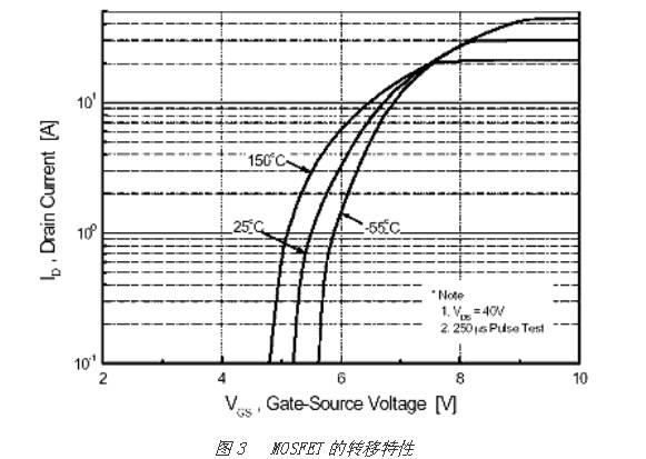
Assuming that the FET current rises to 10 A at turn-on, the gate voltage must transition from 5.2 V to 6.7 V to achieve a value of 10 A according to the curve at 25 ° C in Figure 3 with an average GFS of 10 A / (6.7 V- 5.2V) = 6.7mΩ.

Equation 1 yields the gate drive impedance for the desired on di / dt
Applying the average GFS value to Equation 1 results in a gate drive voltage of Vdrive = 10V, the required di / dt = 600A / μs, FCP11N60 typical values of VGS (avg) = 6V and Ciss = 1200pF; The gate drive impedance is 37Ω. Since the transient GFS value is a diagonal line in the graph of Figure 3, a change occurs during Eon, meaning di / dt also changes. The exponentially decaying gate drive current Vdrive and falling Ciss also enter the formula as a function of VGS, exhibiting an overall effect with surprising linear current rise.
Similarly, similar gate drive on-resistance calculations can be performed for IGBTs. VGE (avg) and GFS can be determined by the IGBT switching characteristics and CIES values at VGE (avg) are used instead of Ciss. Calculated IGBT turn-on gate drive impedance of 100Ω, higher than the previous 37Ω, indicating that IGBT GFS higher CIES lower. The key point here is that in order to switch from the MOSFET to the IGBT, the gate drive circuit must be tuned.
2, conduction loss should be cautious
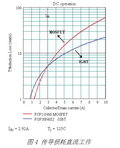
IGBTs typically have less conduction loss than 600 V MOSFETs of the same chip size when compared to devices rated at 600V. Such comparisons should be made when the collector and drain current densities are clearly sensed and at the worst case operating junction temperature. For example, the FGP20N6S2 SMPS2 IGBTs and the FCP11N60 SuperFETs each have a RθJC value of 1 ° C / W. Figure 4 shows the conduction loss versus dc current at a junction temperature of 125 ° C. The plot shows that the conduction loss of the MOSFET is greater at dc currents greater than 2.92A.
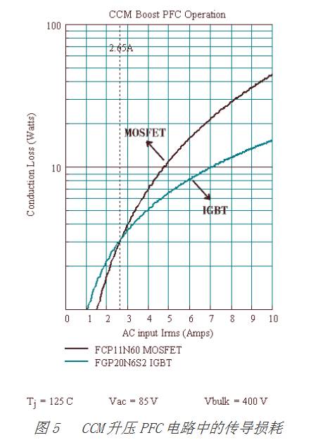
However, the dc conduction losses in Figure 4 are less suitable for most applications. Meanwhile, Figure 5 shows the comparison of conduction losses in CCM (continuous current mode), step-up PFC circuit, junction temperature of 125 ° C, and operating modes of AC input voltage Vac of 85V and DC output voltage of 400 Vdc. In the figure, the curve-crossing point of MOSFET-IGBT is 2.65A RMS. For PFC circuits, MOSFETs have greater conduction losses when the AC input current is greater than 2.65A RMS. The 2.65A PFC AC input current is equal to 2.29A RMS calculated by Equation 2 in the MOSFET. The MOSFET conduction loss, I2R, the current defined by Equation 2, and the RDS (on) of the MOSFET at 125 ° C are calculated. Taking RDS (on) into account for changes in drain current, the conduction loss can be further refined, as shown in Figure 6.
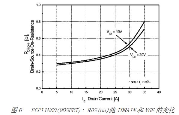
An article entitled How to Include the RDS (on) Power MOSFET's Dependence of Drain Current Transient Values on Conductance Losses in High Frequency Three-Phase PWM Inverters describes how to determine the drain current Effect on conduction loss. As a function of ID, changes in RDS (on) have little effect on most SMPS topologies. For example, in a PFC circuit, when the peak current ID of the FCP11N60 MOSFET is 11 A - twice the 5.5 A specification of the RDS (on) specification, the RDS (on) rms and itw conduction losses Increase by 5%.
In the high-pulsating current topology where MOSFETs conduct very small duty cycles, the characteristics shown in Figure 6 should be considered. If the FCP11N60 MOSFET is operated in a circuit with a drain current of 20A pulses (ie, 5.5A RMS) with a duty cycle of 7.5%, the effective RDS (on) will be less than 5.5A (test current in the datasheet) 0.32 ohm big 25%.

Equation 2 RMS current in the CCM PFC circuit
In Equation 2, Iacrms is the PFC circuit RMS input current; Vac is the PFC circuit RMS input voltage; Vout is the DC output voltage.
In practical applications, calculating the conduction losses of IGBTs in similar PFC circuits will be more complicated because each switching cycle is performed on different ICs. The IGBT's VCE (sat) can not be represented by a single impedance. The simpler, straightforward method is to represent it as a resistor RFCE in series with a fixed VFCE voltage, VCE (ICE) = ICE × RFCE + VFCE. The conduction loss can then be calculated as the product of the average collector current and VFCE, plus the square of the RMS collector current, multiplied by the impedance RFCE.
The example in Figure 5 considers only the conduction loss of the CCM PFC circuit, which is assumed to be less than 15W for the design target with the worst case of conduction. Taking FCP11N60 MOSFET as an example, this circuit is limited to 5.8A, and FGP20N6S2 IGBT can work under 9.8A AC input current. It conducts more than 70% of the MOSFET power.
Although IGBTs have low conduction losses, most 600V IGBTs are PT (Punch Through) devices. PT devices have NTC (negative temperature coefficient) characteristics and can not shunt in parallel. Perhaps, these devices can be paralleled with limited success by matching devices VCE (sat), VGE (TH) (gate firing threshold voltage), and mechanical packages so that the temperature of the IGBT chips can be kept in constant agreement. In contrast, the MOSFET has a PTC (Positive Temperature Coefficient) that provides good current shunting.
3, turn-off loss - the problem is not over
In hard-switched, clamp-inductive circuits, MOSFETs have much lower turn-off losses than IGBTs because of the tailing current of the IGBTs, which is related to the minority carrier removal of the PNP BJTs in Figure 1. Figure 7 shows the function Eoff of collector current ICE and junction temperature Tj, the curves of which are provided in most IGBT datasheets. These curves are based on clamped inductive circuits and have the same test voltage and contain trailing current energy losses.
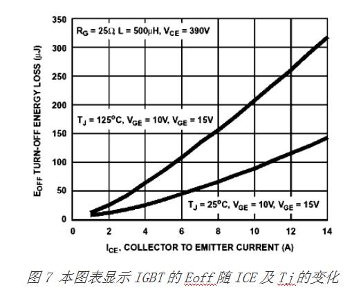
Figure 2 shows a typical test circuit for measuring IGBT Eoff. Its test voltage, VDD in Figure 2, varies with BVCES for different manufacturers and individual devices. The VDD in this test condition should be considered when comparing devices because testing and operation at a lower VDD clamp voltage will result in lower Eoff power consumption.
Reducing the gate drive off resistance has little effect on reducing the IGBT Eoff loss. As shown in Figure 1, there is still a storage time delay td (off) I in the IGBT minority carriers BJT when the equivalent multi-carrier MOSFET is off. However, reducing the Eoff drive impedance will reduce the risk of current injection into the gate drive loop due to Miller capacitance CRES and dv / dt with the VCE turned off, preventing the device from being biased to a conductive state, resulting in Multiple Eoff-generating switching actions.
ZVS and ZCS topologies reduce the turn-off losses of MOSFETs and IGBTs. However, the benefits of ZVS are not so great in IGBTs as the tailing inrush current Eoff is induced when the collector voltage rises to a potential that allows excess stored charge to dissipate. ZCS topology can enhance the maximum IGBT Eoff performance. The correct gate drive sequence allows the IGBT gate signal not to be cleared before the second collector current crosses zero, significantly reducing the IGBT ZCS Eoff.
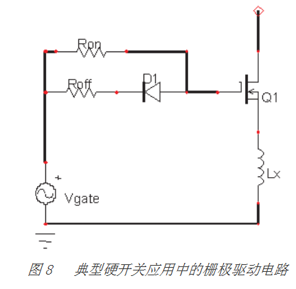
The Eoff energy consumption of a MOSFET is a function of its Miller capacitance Crss, gate drive speed, gate drive off source impedance, and parasitic inductance in the source power circuit path. The circuit parasitic inductance Lx (Figure 8) produces a potential that increases the turn-off loss by limiting the current speed drop. At shutdown, the rate of current drop, di / dt, is determined by Lx and VGS (th). If Lx = 5nH, VGS (th) = 4V, the maximum current drop rate is VGS (th) / Lx = 800A / μs.
There are no comprehensive solutions, circuit topologies, operating frequencies, ambient temperatures, and physical dimensions when choosing power switching devices, all of which play a role in making the best choice.In ZVS and ZCS applications with minimal Eon loss, MOSFETs can operate at higher frequencies due to their faster switching speeds and less switching losses.The recovery behavior of MOSFET parasitic diodes may be a disadvantage for hard switching applications. In contrast, the excellent soft recovery diodes are compatible with higher speed SMPS devices because the diodes in the IGBT package are tailored to specific applications.