


POL regulator is the reason for the heat, because no voltage conversion efficiency can reach 100%. As a result, how much heat will be caused by the package structure, layout, and thermal resistance? The thermal resistance of the package not only increases the temperature of the POL regulator but also increases the temperature of the PCB and surrounding components and makes the system cool Design is more complex. Components installed on the PCB after the elimination of the heat generated by the package there are two main ways:
1) When using the surface mount method, the heat conduction to the copper PCB layer, from the bottom of the package heat.
2) radiating heat from the top of the package with cold airflow, or, more precisely, the heat is transferred to air molecules that are in contact with the top surface of the package, at lower temperatures and faster.
Of course, there are some passive and active cooling methods, for the sake of simplicity, we classify these methods into the second category. Therefore, from the perspective of thermal management, to keep the entire system, including DC / DC POL regulators running in a safe temperature range, more copper PCB layer, larger PCB area, thicker PCB Layer, decentralized components on the PCB, larger and faster fans are so good ideas. Good idea is a good idea, but the small, high-power POL regulator for heat management, whether there are other helpful methods?
Although some or all of the above methods are effective for limiting system heat, the use of these thermal methods may make the system or the final product out of competitive advantage. The final product (such as a router) may become too large by deliberately expanding the distance between the components on the PCB, resulting in an increase in audible noise due to the increase in the number of fans and the rapid flow of air into and out of the heat, which may eventually The final product becomes inferior products on the market, because in order to win in the competition, companies are constantly in the compact, computing power, data transmission rate, efficiency, cooling costs and so on to make improvements. 28nm, 20nm and lower than 20nm digital devices to provide higher performance, but greater power consumption, and equipment suppliers with faster, smaller, lower noise, more efficient innovation Competition. The new digital technology is superior and exciting, but there are still simulation and power technologies behind it to provide greater power in smaller packages while minimizing the overall temperature of the system. The POL regulator with a higher power density seems to be a good choice: this regulator is smaller but larger in power.
Through the power density numerical decision POL regulator is suitable for ... ... for the novice
The POL regulator per square (or cubic) 40W of the POL regulator should be better than the 30W regulator per square centimeter. Vendors use power density to sell products, the system designer's power density requirements for the regulator year by year to rely on the next version faster, smaller, lower noise, more efficient products and rival competition. In the choice of "better" POL regulator, the higher power density value is the decisive factor? We from the following aspects to consider this issue.
First, put the power density on the side, look at the POL regulator data sheet. Find the calorie derating curve. Describe the detailed POL regulator data sheet There should be many such curves that specify the output current, output voltage, and airflow speed for different input voltages, output voltages, and airflow speeds, respectively. In other words, such a data sheet should show the output current capability of the POL regulator under specific circuit conditions so that the designer can determine whether it is suitable for the heat and load current capability of the regulator. Is the regulator meeting the typical and maximum ambient temperature and airflow speed requirements of the system? Remember that the output current derating is related to the thermal performance of the device. These two factors are closely related and equally important.
Followed by efficiency, efficiency is not the first, but in the second. The efficiency of a single DC / DC regulator is not accurate. Also need to calculate the input current and load current, input power consumption, power consumption, junction temperature ... and so on. However, in order to better illustrate the problem, the efficiency value should be studied while considering the output current derating and other heat data related to the device and its package. For example, a 98% efficiency DC / DC buck converter will leave a very deep impression. Even more amazing is that this converter also claims to have excellent power density values. Will you buy this device?
A seasoned engineer should ask 2% of the efficiency of the loss of any impact. How is this efficiency loss converted to a rise in package temperature? What is the junction temperature of this high power density and high efficiency regulator at ambient temperatures of 60 ° C and 200LFM airflow? To break the typical value at room temperature of 25 ° C Think about the problem. What is the maximum and minimum values measured at extreme temperatures of 40 ° C, 85 ° C or 125 ° C? What if the package thermal resistance is too high and the junction temperature rises above the safe operating temperature range? Expensive voltage regulator must be reduced to a very low output current value, then the output power will not be reduced due to the high price of the device is no longer reasonable?
The last factor to consider is whether this POL regulator is easy to cool. The package thermal resistance values provided in the data sheet are key data for simulating and calculating the junction temperature, ambient temperature, and housing temperature rise of the device. Since most of the heat in the surface mount package is diffused from the bottom of the package to the PCB, the layout guidelines and various heat measurement conditions and methods must be specified in the data sheet to avoid accidental formation of subsequent prototype systems.
A well-designed package should be able to efficiently dissipate heat through all package surfaces to eliminate heat concentration problems and hot spots that can reduce the reliability of POL regulators and should be eliminated or mitigated. As mentioned earlier, PCBs are responsible for absorbing the heat of the surface-mount POL regulators and providing a thermal path, but in today's dense and complex systems, airflow is common, so a more intelligent POL regulator Utilize this "free" cooling opportunity to remove heat from heat generating components such as MOSFETs and inductors.
Heat the heat from the inside of the package to the top of the package and diffuse into the air
The high power switch POL regulator converts the input supply voltage to a stable output voltage by an inductor or transformer. The non-isolated, step-down type POL regulator uses an inductor, which induces the heat generated by the switching components such as MOSFETs during DC / DC conversion. About 10 years ago, due to the advances in LED packaging technology, the entire DC / DC regulator circuit, including magnetic components, could be housed in a molded plastic package called a module or SiP, a molded plastic package that produced large Part of the heat must be guided from the bottom of the package to the PCB. Any conventional method of increasing the heat dissipation capability of the package will result in a larger package, such as a radiator attached to the top of the surface mount package.
However, three years ago there was an innovative modular packaging method that utilizes the available airflow to achieve device cooling. The radiator is integrated into the module package and is fully molded. The radiator is unique in shape, one end in the package connected to the heat source MOSFET and inductor, the other end is a flat surface, exposed to the top of the package. With this new package and built-in heatsink technology, the device can be cooled quickly with some airflow because the flat radiator surface is in contact with air at the top of the package and air can take heat from the top of the package (see TechClip video Of the LTM4620 data sheet). Another way to improve the thermal performance of high-power POL regulators has pushed this approach forward a step forward.
To replace the inductor as a radiator POL module regulator
The size of the inductor in the POL regulator depends on many factors, including voltage, switching frequency, current to be processed and its structure. When a modular approach is adopted, the DC / DC circuit that includes the inductor is fully molded and sealed in a plastic package that looks like an IC. The size of the inductor determines the thickness, volume, and weight of the package. The inductor is also a heating element that increases the internal temperature of the POL module regulator. The previously discussed approach, that is, integrating the heatsink in the package to transfer the heat from the MOSFET and the inductor to the top of the package, is very useful for quickly passing the heat inside the package from the top of the package to the outside of the package and ultimately to In the air, this radiator is a cooling plate or passive radiator. However, this method is suitable for inductors with small size and current, which is easy to fit into a plastic molded package. The larger POL regulators need to use inductors with larger size and current. Putting these magnetic components into the package will cause the other components of the circuit to be pushed aside, thus increasing the footprint of the package Of the area. A larger footprint means a heavier package. In order to maintain a smaller footprint and further improve heat dissipation, packaging engineers have developed another approach: vertical, stacked or 3D package (Figure 1).
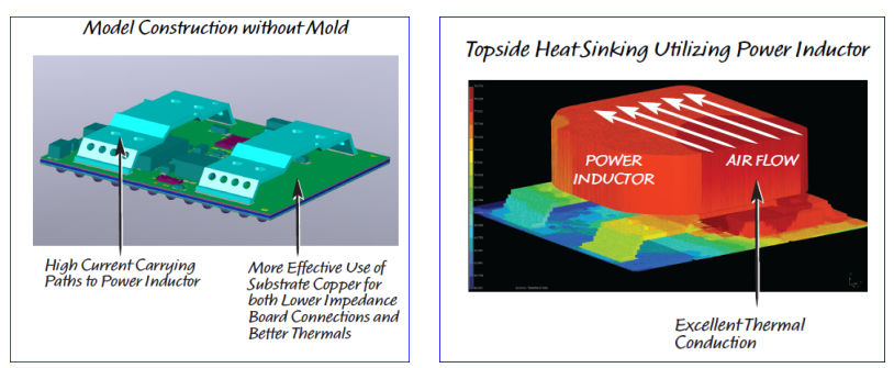
Figure 1: 3D or vertical packaging technology for high-power POL regulator modules increases the placement of the inductor as a radiator in the airflow. The rest of the DC / DC circuit is mounted in the substrate underneath the inductor so that the package occupies a smaller PCB area and improves its thermal performance.
Model Construction without Mold: Unmodified model structure
High Current Carrying Paths to Power Inductor: A high current path into the power inductor
More Effective Use of Substrate Copper for both Lower Impedance Board Connections and Better Thermals: More Efficient Use of Copper Substrates to Reduce Board Connection Impedance and Improve Heat Dissipation
Topside Heat Sinking Utilizing Power Inductor: Place the power inductor on top of the package
POWER INDUCTOR: Power inductor
AIRFLOW: airflow
Excellent thermal Conduction: Excellent heat conduction
3D package with bare overlay inductor: small footprint, improved power, improved heat dissipation
Using 3D packaging This new method of constructing a POL regulator can achieve three advantages of small footprint, higher power and higher thermal performance (Figure 1 and Figure 2). The LTM4636 is a μModule regulator with built-in DC / DC regulator IC, MOSFET, support circuit and a large inductor that reduces output ripple and provides up to 40A of load current from The 12V input provides an accurate and stable 3.3V to 0.6V output voltage. Four LTM4636 devices can divide the current to provide 160A load current. The device footprint is only 16mm x 16mm. If you calculate, the power density is very high. However, remember not to be fooled by numbers. For system designers, the benefits of this μModule regulator are thermal performance, as well as impressive DC / DC conversion efficiency and cooling capacity.
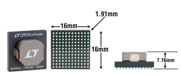
Figure 2: LTM4636 with a stacked inductor as a radiator, with a small footprint area to achieve an impressive thermal performance
In order to maintain a small footprint (16mm x 16mm BGA), the area of the inductor with a large area of the board is raised and placed on the two wireframes so that the remaining circuit components (diodes, resistors, MOSFET, capacitor, DC / DC IC) can be soldered to the substrate underneath the inductor. If the inductor is placed on the substrate, then the μModule regulator can easily take up more than 1225 square millimeters of PCB area instead of the current 256 square millimeters. This approach allows the system designer to design a more compact POL regulator layout, but the method also has a very big advantage, it can achieve good thermal performance.
The stacked inductors in the LTM4636 are not molded (sealed) with the plastic package. The rest of the components are molded. The inductor has a sleek corner and the structure is raised to allow it to be exposed to the air, and the air is more likely to flow around it and the upper part (the flow resistance is minimal).
The value reflected in the fact: 40A LTM4636 thermal performance and efficiency
The LTM4636 is a 40A μModule regulator with 3D packaging technology, also known as Component-on-Package (CoP, Figure 2). The device is packaged in a fully molded 16mm x 16mm x 1.91mm BGA package. With the inductor mounted on top of the molded package, the LTM4636's overall package height is from the bottom of the BGA solder ball (144) to the top of the inductor at a height of 7.16mm.
In addition to cooling from the top, the LTM4636 can efficiently transfer heat from the bottom of the package to the PCB. The device has 144 BGA solder balls, these solder balls are arranged in rows to connect to a large current flowing through the GND, VIN and VOUT. These solder balls combine to act as heat sinks that transfer heat to the PCB. The LTM4636 is optimized for cooling from the top and bottom of the package.
The LTM4636 is only 40 ° C above ambient temperature (25 ° C to 26.5 ° C) at 12VIN, 1VOUT, 40A (40W) full load current and standard 200LFM airflow. Figure 3 shows the thermal image of the LTM4636 under the above conditions. Figure 4 below shows the derating value. At 200LFM, the LTM4636 provides a maximum current of 40A at ambient temperatures up to 83 ° C. At ambient temperatures up to 110 ° C, half of the maximum current (ie 20A) can be provided. This means that the ability of the LTM4636 to provide load current is less affected by ambient temperature when there is airflow.
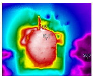
Figure 3: Temperature rises by only 40 ° C at 40W (12VIN to 1VOUT, 40A, 200LFM)
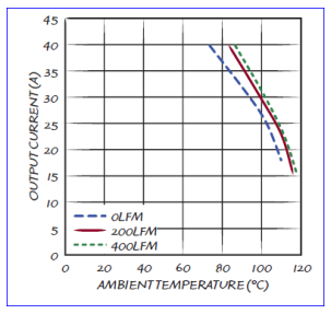
Figure 4: 200LFM, 83 ° C ambient temperature to provide 40A maximum current
OUTPUT CURRENT: Output current
AMBIENT TEMPERATURE: Ambient temperature
MOSFET performance is best and DC / DC controller strong driver is the LTM4636 conversion efficiency is high reason. The following is the 12Vin power supply step-down conversion of some of the figures: 3.3V, 25A when the efficiency of 95%, 1.8V, 40A when the efficiency of 93%, 1V, 40A when the efficiency of 88%. Figure 5 summarizes the efficiency figures from 12Vin to 1Vout to 3.3Vout.
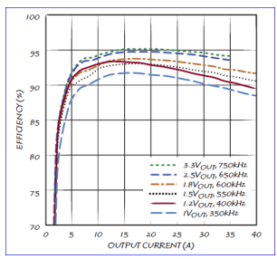
Figure 5: DC / DC conversion with high efficiency when switching from 12VIN to various output voltages
EFFICIENCY: Efficiency
OUTPUT CURRENT: Output current
With a thermal balance of 160W, scalable 4 x 40A μModule POL regulator
The load current rating of an LTM4636 is 40A. Two LTM4636s with current equalization mode (or parallel) provide 80A current and four LTM4636s provide 160A current (Figure 6 and Figure 7). The LTM4636's current-mode architecture allows accurate division of current across multiple 40A modules. Accurate current equalization allows balanced heat dissipation between two, three or four parallel devices (Figures 6 and 7). Because of this balance of heat dissipation, so no one device will be overloaded or overheated. Another feature of this device is the ability to run out of phase to reduce the output and input ripple current, which reduces the number of input and output capacitors. For example, four LTM4636s run at 90 ° (360 ° ÷ 4). The device also provides clock and phase control functions. In addition, the layout required to increase the power of the work is very simple, just copy and paste the board area can be (symbol and footprint area available).
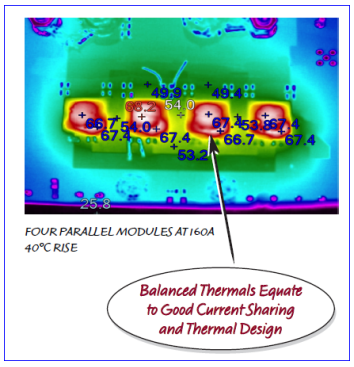
Figure 6: Accurate current equalization enables four parallel LTM4636s to balance heat dissipation. Harvatek rises by only 40 ° C at 12VIN, 1VOUT, 160A, 400LFM
FOUR PARALLEL MODULES AT 160A 40 ° C RISE: 4 parallel modules, 160A current, temperature rise 40 ° C
Balanced Thermals Equate to Good Current Sharing and Thermal Design: Good current sharing and thermal design equals balanced heat dissipation
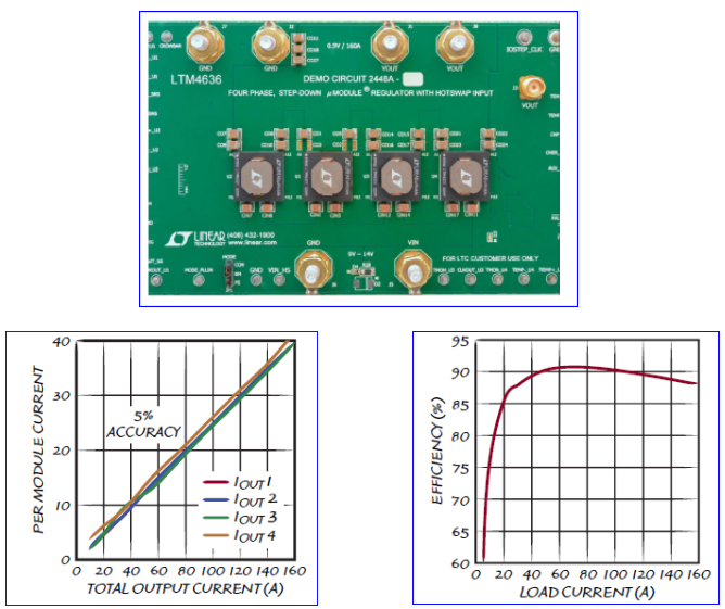
Figure 7: 4 parallel LTM4636 each with a precise current sharing capability and high efficiency, 12VIN to 0.9VOUT, 160A
PER MODULE CURRENT: Current per module
ACCURACY: Accuracy
TOTAL OUTPUT CURRENT: Total output current
EFFICIENCY: Efficiency
LOAD CURRENT: Load current
1) When using the surface mount method, the heat conduction to the copper PCB layer, from the bottom of the package heat.
2) radiating heat from the top of the package with cold airflow, or, more precisely, the heat is transferred to air molecules that are in contact with the top surface of the package, at lower temperatures and faster.
Of course, there are some passive and active cooling methods, for the sake of simplicity, we classify these methods into the second category. Therefore, from the perspective of thermal management, to keep the entire system, including DC / DC POL regulators running in a safe temperature range, more copper PCB layer, larger PCB area, thicker PCB Layer, decentralized components on the PCB, larger and faster fans are so good ideas. Good idea is a good idea, but the small, high-power POL regulator for heat management, whether there are other helpful methods?
Although some or all of the above methods are effective for limiting system heat, the use of these thermal methods may make the system or the final product out of competitive advantage. The final product (such as a router) may become too large by deliberately expanding the distance between the components on the PCB, resulting in an increase in audible noise due to the increase in the number of fans and the rapid flow of air into and out of the heat, which may eventually The final product becomes inferior products on the market, because in order to win in the competition, companies are constantly in the compact, computing power, data transmission rate, efficiency, cooling costs and so on to make improvements. 28nm, 20nm and lower than 20nm digital devices to provide higher performance, but greater power consumption, and equipment suppliers with faster, smaller, lower noise, more efficient innovation Competition. The new digital technology is superior and exciting, but there are still simulation and power technologies behind it to provide greater power in smaller packages while minimizing the overall temperature of the system. The POL regulator with a higher power density seems to be a good choice: this regulator is smaller but larger in power.
Through the power density numerical decision POL regulator is suitable for ... ... for the novice
The POL regulator per square (or cubic) 40W of the POL regulator should be better than the 30W regulator per square centimeter. Vendors use power density to sell products, the system designer's power density requirements for the regulator year by year to rely on the next version faster, smaller, lower noise, more efficient products and rival competition. In the choice of "better" POL regulator, the higher power density value is the decisive factor? We from the following aspects to consider this issue.
First, put the power density on the side, look at the POL regulator data sheet. Find the calorie derating curve. Describe the detailed POL regulator data sheet There should be many such curves that specify the output current, output voltage, and airflow speed for different input voltages, output voltages, and airflow speeds, respectively. In other words, such a data sheet should show the output current capability of the POL regulator under specific circuit conditions so that the designer can determine whether it is suitable for the heat and load current capability of the regulator. Is the regulator meeting the typical and maximum ambient temperature and airflow speed requirements of the system? Remember that the output current derating is related to the thermal performance of the device. These two factors are closely related and equally important.
Followed by efficiency, efficiency is not the first, but in the second. The efficiency of a single DC / DC regulator is not accurate. Also need to calculate the input current and load current, input power consumption, power consumption, junction temperature ... and so on. However, in order to better illustrate the problem, the efficiency value should be studied while considering the output current derating and other heat data related to the device and its package. For example, a 98% efficiency DC / DC buck converter will leave a very deep impression. Even more amazing is that this converter also claims to have excellent power density values. Will you buy this device?
A seasoned engineer should ask 2% of the efficiency of the loss of any impact. How is this efficiency loss converted to a rise in package temperature? What is the junction temperature of this high power density and high efficiency regulator at ambient temperatures of 60 ° C and 200LFM airflow? To break the typical value at room temperature of 25 ° C Think about the problem. What is the maximum and minimum values measured at extreme temperatures of 40 ° C, 85 ° C or 125 ° C? What if the package thermal resistance is too high and the junction temperature rises above the safe operating temperature range? Expensive voltage regulator must be reduced to a very low output current value, then the output power will not be reduced due to the high price of the device is no longer reasonable?
The last factor to consider is whether this POL regulator is easy to cool. The package thermal resistance values provided in the data sheet are key data for simulating and calculating the junction temperature, ambient temperature, and housing temperature rise of the device. Since most of the heat in the surface mount package is diffused from the bottom of the package to the PCB, the layout guidelines and various heat measurement conditions and methods must be specified in the data sheet to avoid accidental formation of subsequent prototype systems.
A well-designed package should be able to efficiently dissipate heat through all package surfaces to eliminate heat concentration problems and hot spots that can reduce the reliability of POL regulators and should be eliminated or mitigated. As mentioned earlier, PCBs are responsible for absorbing the heat of the surface-mount POL regulators and providing a thermal path, but in today's dense and complex systems, airflow is common, so a more intelligent POL regulator Utilize this "free" cooling opportunity to remove heat from heat generating components such as MOSFETs and inductors.
Heat the heat from the inside of the package to the top of the package and diffuse into the air
The high power switch POL regulator converts the input supply voltage to a stable output voltage by an inductor or transformer. The non-isolated, step-down type POL regulator uses an inductor, which induces the heat generated by the switching components such as MOSFETs during DC / DC conversion. About 10 years ago, due to the advances in LED packaging technology, the entire DC / DC regulator circuit, including magnetic components, could be housed in a molded plastic package called a module or SiP, a molded plastic package that produced large Part of the heat must be guided from the bottom of the package to the PCB. Any conventional method of increasing the heat dissipation capability of the package will result in a larger package, such as a radiator attached to the top of the surface mount package.
However, three years ago there was an innovative modular packaging method that utilizes the available airflow to achieve device cooling. The radiator is integrated into the module package and is fully molded. The radiator is unique in shape, one end in the package connected to the heat source MOSFET and inductor, the other end is a flat surface, exposed to the top of the package. With this new package and built-in heatsink technology, the device can be cooled quickly with some airflow because the flat radiator surface is in contact with air at the top of the package and air can take heat from the top of the package (see TechClip video Of the LTM4620 data sheet). Another way to improve the thermal performance of high-power POL regulators has pushed this approach forward a step forward.
To replace the inductor as a radiator POL module regulator
The size of the inductor in the POL regulator depends on many factors, including voltage, switching frequency, current to be processed and its structure. When a modular approach is adopted, the DC / DC circuit that includes the inductor is fully molded and sealed in a plastic package that looks like an IC. The size of the inductor determines the thickness, volume, and weight of the package. The inductor is also a heating element that increases the internal temperature of the POL module regulator. The previously discussed approach, that is, integrating the heatsink in the package to transfer the heat from the MOSFET and the inductor to the top of the package, is very useful for quickly passing the heat inside the package from the top of the package to the outside of the package and ultimately to In the air, this radiator is a cooling plate or passive radiator. However, this method is suitable for inductors with small size and current, which is easy to fit into a plastic molded package. The larger POL regulators need to use inductors with larger size and current. Putting these magnetic components into the package will cause the other components of the circuit to be pushed aside, thus increasing the footprint of the package Of the area. A larger footprint means a heavier package. In order to maintain a smaller footprint and further improve heat dissipation, packaging engineers have developed another approach: vertical, stacked or 3D package (Figure 1).
Figure 1: 3D or vertical packaging technology for high-power POL regulator modules increases the placement of the inductor as a radiator in the airflow. The rest of the DC / DC circuit is mounted in the substrate underneath the inductor so that the package occupies a smaller PCB area and improves its thermal performance.
Model Construction without Mold: Unmodified model structure
High Current Carrying Paths to Power Inductor: A high current path into the power inductor
More Effective Use of Substrate Copper for both Lower Impedance Board Connections and Better Thermals: More Efficient Use of Copper Substrates to Reduce Board Connection Impedance and Improve Heat Dissipation
Topside Heat Sinking Utilizing Power Inductor: Place the power inductor on top of the package
POWER INDUCTOR: Power inductor
AIRFLOW: airflow
Excellent thermal Conduction: Excellent heat conduction
3D package with bare overlay inductor: small footprint, improved power, improved heat dissipation
Using 3D packaging This new method of constructing a POL regulator can achieve three advantages of small footprint, higher power and higher thermal performance (Figure 1 and Figure 2). The LTM4636 is a μModule regulator with built-in DC / DC regulator IC, MOSFET, support circuit and a large inductor that reduces output ripple and provides up to 40A of load current from The 12V input provides an accurate and stable 3.3V to 0.6V output voltage. Four LTM4636 devices can divide the current to provide 160A load current. The device footprint is only 16mm x 16mm. If you calculate, the power density is very high. However, remember not to be fooled by numbers. For system designers, the benefits of this μModule regulator are thermal performance, as well as impressive DC / DC conversion efficiency and cooling capacity.
Figure 2: LTM4636 with a stacked inductor as a radiator, with a small footprint area to achieve an impressive thermal performance
In order to maintain a small footprint (16mm x 16mm BGA), the area of the inductor with a large area of the board is raised and placed on the two wireframes so that the remaining circuit components (diodes, resistors, MOSFET, capacitor, DC / DC IC) can be soldered to the substrate underneath the inductor. If the inductor is placed on the substrate, then the μModule regulator can easily take up more than 1225 square millimeters of PCB area instead of the current 256 square millimeters. This approach allows the system designer to design a more compact POL regulator layout, but the method also has a very big advantage, it can achieve good thermal performance.
The stacked inductors in the LTM4636 are not molded (sealed) with the plastic package. The rest of the components are molded. The inductor has a sleek corner and the structure is raised to allow it to be exposed to the air, and the air is more likely to flow around it and the upper part (the flow resistance is minimal).
The value reflected in the fact: 40A LTM4636 thermal performance and efficiency
The LTM4636 is a 40A μModule regulator with 3D packaging technology, also known as Component-on-Package (CoP, Figure 2). The device is packaged in a fully molded 16mm x 16mm x 1.91mm BGA package. With the inductor mounted on top of the molded package, the LTM4636's overall package height is from the bottom of the BGA solder ball (144) to the top of the inductor at a height of 7.16mm.
In addition to cooling from the top, the LTM4636 can efficiently transfer heat from the bottom of the package to the PCB. The device has 144 BGA solder balls, these solder balls are arranged in rows to connect to a large current flowing through the GND, VIN and VOUT. These solder balls combine to act as heat sinks that transfer heat to the PCB. The LTM4636 is optimized for cooling from the top and bottom of the package.
The LTM4636 is only 40 ° C above ambient temperature (25 ° C to 26.5 ° C) at 12VIN, 1VOUT, 40A (40W) full load current and standard 200LFM airflow. Figure 3 shows the thermal image of the LTM4636 under the above conditions. Figure 4 below shows the derating value. At 200LFM, the LTM4636 provides a maximum current of 40A at ambient temperatures up to 83 ° C. At ambient temperatures up to 110 ° C, half of the maximum current (ie 20A) can be provided. This means that the ability of the LTM4636 to provide load current is less affected by ambient temperature when there is airflow.
Figure 3: Temperature rises by only 40 ° C at 40W (12VIN to 1VOUT, 40A, 200LFM)
Figure 4: 200LFM, 83 ° C ambient temperature to provide 40A maximum current
OUTPUT CURRENT: Output current
AMBIENT TEMPERATURE: Ambient temperature
MOSFET performance is best and DC / DC controller strong driver is the LTM4636 conversion efficiency is high reason. The following is the 12Vin power supply step-down conversion of some of the figures: 3.3V, 25A when the efficiency of 95%, 1.8V, 40A when the efficiency of 93%, 1V, 40A when the efficiency of 88%. Figure 5 summarizes the efficiency figures from 12Vin to 1Vout to 3.3Vout.
Figure 5: DC / DC conversion with high efficiency when switching from 12VIN to various output voltages
EFFICIENCY: Efficiency
OUTPUT CURRENT: Output current
With a thermal balance of 160W, scalable 4 x 40A μModule POL regulator
The load current rating of an LTM4636 is 40A. Two LTM4636s with current equalization mode (or parallel) provide 80A current and four LTM4636s provide 160A current (Figure 6 and Figure 7). The LTM4636's current-mode architecture allows accurate division of current across multiple 40A modules. Accurate current equalization allows balanced heat dissipation between two, three or four parallel devices (Figures 6 and 7). Because of this balance of heat dissipation, so no one device will be overloaded or overheated. Another feature of this device is the ability to run out of phase to reduce the output and input ripple current, which reduces the number of input and output capacitors. For example, four LTM4636s run at 90 ° (360 ° ÷ 4). The device also provides clock and phase control functions. In addition, the layout required to increase the power of the work is very simple, just copy and paste the board area can be (symbol and footprint area available).
Figure 6: Accurate current equalization enables four parallel LTM4636s to balance heat dissipation. Harvatek rises by only 40 ° C at 12VIN, 1VOUT, 160A, 400LFM
FOUR PARALLEL MODULES AT 160A 40 ° C RISE: 4 parallel modules, 160A current, temperature rise 40 ° C
Balanced Thermals Equate to Good Current Sharing and Thermal Design: Good current sharing and thermal design equals balanced heat dissipation
Figure 7: 4 parallel LTM4636 each with a precise current sharing capability and high efficiency, 12VIN to 0.9VOUT, 160A
PER MODULE CURRENT: Current per module
ACCURACY: Accuracy
TOTAL OUTPUT CURRENT: Total output current
EFFICIENCY: Efficiency
LOAD CURRENT: Load current