


How to test the polarity of IGBT?
1.determine the polarity first multimeter dial in the R & TImes; 1KQ file, with a multimeter measurement, if a pole and other two pole resistance is infinite, after changing the test pen and the other two poles of the resistance is still infinite, then judge this Extremely gate (G). The remaining two poles are then measured with a multimeter. If the measured resistance is infinite, change the meter to measure the resistance. In the measurement of a small resistance value, it is determined that the red pen is a collector (C): the black pen is an emitter (E).
2. To judge the quality, set the multimeter to the R&TImes;10KQ file, connect the collector of the IGBT (C) with a black pen, and connect the red pen to the time of the IGBT (E). At this time, the pointer of the multimeter is at zero. Touching the gate (G) and the collector (C) at the same time with your finger, the GBT is triggered to conduct. The pointer of the multimeter swings to a direction with a smaller resistance, and the station can indicate a certain position. Then touch the gate (G) and emitter (E) at the same time with your fingers. The IGBT is then blocked and the multimeter's hands are homed. At this point, it can be judged that the IGBT is good.
3. Notice Any pointer type multimeter bell can be used to detect IGBT. Note that when judging the IGBT is good or bad, be sure to set the multimeter to R&TImes;IOK block, because R&TImes; IKQ file below each file multimeter internal battery voltage is too low, the IGBT can not be turned on when the test is good or bad, and can not judge the IGBT is good or bad . This method can also be used to detect the quality of power field effect transistors (P-MOSFETs).
4. The quality of the IGBT tube can be detected by the Rxlk block of the multimeter, or by using the “diode” block of the digital multimeter to measure the forward voltage drop of the PN junction. Shortly discharge the three pins of the IGBT tube before testing to avoid affecting the accuracy of the test. Then use the two multimeters of the multimeter to measure the resistances of the G and e poles and the G and C poles. For normal IGBTs (normal The forward and reverse resistances between the G and C poles and the G and C poles are infinity; the IGBTs with the damper diodes are normal, and there are 4kΩ forward resistances between the e and C poles. The above measured values are infinite. ; Finally, with a pointer multimeter red pen then c pole, black pen then e pole, if the measured value in 3. About 5kΩ l, the measured tube is an IGBT tube with a damped diode. If the measured value is about 50kΩ, the measured IGBT tube does not contain a damper diode. For digital multimeters, under normal conditions, the forward voltage drop between the C and C poles of the IGBT tube is approximately zero. 5V.
IGBT package flow and its principle analysis:
The IGBT module package integrates multiple IGBTs together to improve the service life and reliability of the IGBT module. The smaller size, higher efficiency, and higher reliability are the market's demand for IGBT modules. This requires IGBTs. Module packaging technology development and application. Currently popular IGBT module package types are lead type, solder pin type, flat type, and disc type. There are many common module packaging technologies, and each manufacturer's name is different, such as Infineon's 62mm package, TP34 , DP70 and so on.
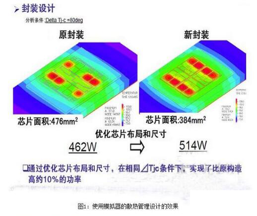
The IGBT module has three connection parts: an aluminum wire bonding point on a silicon wafer, a soldering surface of a silicon wafer and a ceramic insulating substrate, a soldering surface of a ceramic insulating substrate and a copper substrate. The damage of these joints is caused by the stress caused by the mismatch of the thermal expansion coefficients (C violations) of the two materials at the contact surface and the thermal deterioration of the material. Thermal management design, through the use of packaged thermal simulation technology, optimizes the chip layout and size, so under the same ΔTjc conditions, successfully achieved about 10% higher output power than the original.
There are many IGBT module packaging technologies, but they are nothing more than thermal management design, ultrasonic terminal welding technology, and highly reliable soldering technology. The following describes the principles and features of the three technologies in the Fujitsu classic IGBT package, PrimePACK:
(1) In terms of thermal management design, the chip layout and dimensions were optimized through the use of packaged thermal simulation technology, which resulted in an output power that was about 10% higher than the original under the same ΔTjc condition. Thermal management design, through the use of packaged thermal simulation technology, optimizes the chip layout and size, so under the same ΔTjc conditions, successfully achieved about 10% higher output power than the original.
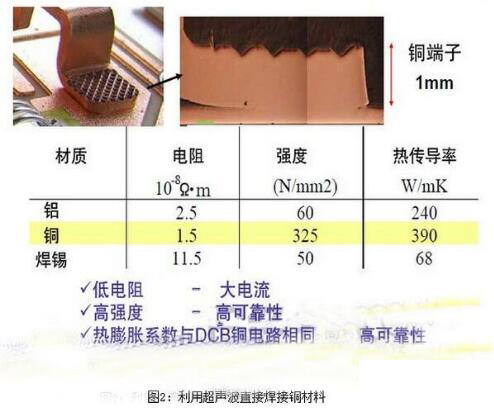
(2) Ultrasonic terminal soldering technology It is possible to directly solder the copper pads connected with the soldering method to copper bonding wires (Fig. 2). Compared with the soldering method, this technology not only has a high melting point and high strength, but also does not have a linear expansion coefficient difference, and can obtain high reliability (Figure 3). Participants do not need special preparation for using this technology. Fuji has been manufacturing in an environment that is nearly vacuum-free in an ordinary dust-free room. This method does not have much problem.
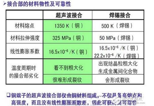
Figure 3: Comparison of ultrasonic welding and soldering
(3) High reliability soldering technology. Normal Sn-Ag welding reduces the strength by 35% after 300 temperature cycles, while Sn-Ag-In and Sn-Sb welding do not decrease in strength after the same cycle. These technologies all have "high temperature reliability."
IGBT module packaging process: a welding - a state line - secondary welding - secondary wire - assembly - upper shell, sealant - curing - silicone gel - aging screening . These processes are not solid, depending on the specific module, some may not require multiple welding or bonding, some may need, and some may have other processes. The above are just some of the major process processes, there are other auxiliary processes, such as plasma processing, ultrasonic scanning, testing, marking and so on.
The role of IGBT module packaging IGBT module packaging uses a gel isolation technology to prevent the explosion during operation; second is the electrode structure uses a spring structure, can ease the formation of cracks on the substrate during the installation process, resulting in cracks in the substrate; the third is The bottom plate is processed and designed so that the bottom plate is in close contact with the radiator, which improves the thermal cycle capability of the module. The design of the bottom plate is to use the middle point design. Under our specified installation conditions, its amplitude will disappear and a better connection with the heat sink will be achieved. After the installation process we see that it plays a role in the installation process. Product performance, we use the IGBT process, the open process for the IGBT is relatively modest, the shutdown process is more demanding. Most of the damage is caused by the shutdown exceeding the rated value.
Detailed technical description of IGBT module packaging process
The first point is about welding technology. If we want to achieve a good thermal conductivity, when we perform chip welding and perform DBC substrate welding, the welding quality directly affects the heat transfer during operation. From the above structure diagram we can see the welding achieved by vacuum welding technology. You can see the void ratio of DBC and substrate. This will not result in heat buildup and will not damage the IGBT module.
The second is bonding technology. The bonding technology used by Fujitsu is ultrasonic bonding. Deformation of data. The main effect of bonding is to achieve electrical connections. In the case of currents of 600 A and 1200 Am, all currents are realized by the IGBT, and the length of the bond is very important. The size of the module is determined by the size of the recessed current and the size of the current. During the application process, if the bond is stuck and the length is improper, the current distribution will be uneven and the IGBT module will be easily damaged. The installation of the shell, because the IGBT itself is not directly with the air and other environmental contact, to achieve insulation performance, mainly through the shell to achieve. The enclosure requires that it be resistant to high temperatures, non-deformable, moisture-proof, and corrosion-resistant in terms of material selection.
The fourth is the tank sealing technology. If IGBTs are used on high-speed rail, trains and locomotives, the environment of the locomotives and vehicles is very bad. We may encounter wet weather, high humidity, high altitude, or relatively large dust. The isolation between the IGBT chip and the external environment is achieved, and the reliability of the operation is well achieved. Its potting material plays an important role. It requires the use of materials with stable, non-corrosive properties, insulation, heat dissipation, and low expansion ratio and low shrinkage. When we mass-encapsulate, the part of the filling material is added into the buffer layer, and the chip is heated and cooled during operation. If the thermal expansion coefficient of the filler material is not consistent with the shell during this process, it may cause delamination. Adding a filler similar to the buffering function in the middle of the IGBT module can prevent delamination.
The fifth is the quality control link. Quality control All high-power IGBTs after completion of production need to be tested on all aspects of performance. This is also the basis of quality assurance. It is possible to test the flatness of the backplane through planar facilities, and the flatness is in the IGBT. After installation, all heat is transferred to the radiator from the backplane. The better the flatness, the better the heat sink contact performance and the better the thermal conductivity. The second is a push-pull test that tests the strength of the bonding point. The third hardness tester, the hardness of the main electrode, can not be too hard, nor too soft. Ultrasonic scanning mainly scans the welding process and the porosity of the product after welding. This is also a good control of thermal conductivity. IGBT module electrical aspects of monitoring methods, mainly to monitor the IGBT module, its parameters, characteristics can meet our design requirements, the second insulation test.