


In the day-to-day work, electronic engineers will come into contact with various types of ICs, such as logic chips, memory chips, MCUs, or FPGAs. For their functional characteristics, engineers may be more clear, but do not know Understand how many? Here will introduce some of the commonly used IC packaging principles and functional characteristics, by understanding the various types of IC packaging, electronic engineers in the design of electronic circuit principle, you can accurately select the IC, and for the factory mass production burn, but also Quickly find the corresponding IC package burner model.
一、 DIP dual in-line package
DIP refers to the use of dual in-line package of integrated circuit chip, the vast majority of small and medium-sized integrated circuits (IC) are used in this form of packaging, the pin count is generally not more than 100. The ICs with DIP packages have two rows of pins that need to be plugged into a chip socket with DIP structure. Of course, can also be directly inserted in the same number of holes and geometric arrangement of the circuit board for welding. DIP-packaged chips should be handled with care when removing the pins from the chip receptacle to avoid damage to the pins.
DIP package has the following characteristics:
1、suitable for PCB (printed circuit board) on the perforated welding, easy to operate.
2、 the chip area and the ratio between the packaging area is larger, so the volume is also larger.
3、DIP is the most popular plug-in package, the scope of application, including standard logic IC, memory and microcomputer circuits.
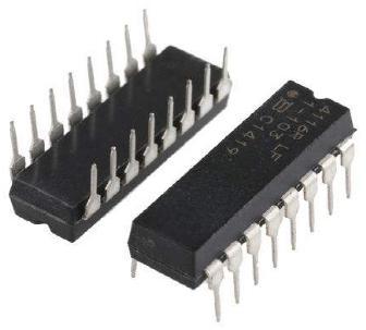
Figure 1 DIP package diagram
二、QFP / PFP type package
QFP / PFP package chip pin between the small distance, the pin is very fine, the general large-scale or very large integrated circuits are used in this form of packaging. Chip encapsulated in this form must be SMD (surface mount device technology) to chip and motherboard welding. SMD installed with the chip does not have to punch on the motherboard, generally on the surface of the motherboard has a good design of the corresponding pin of the solder joints. The chip feet at the corresponding solder joints, you can achieve with the motherboard welding.
The QFP / PFP package has the following features:
1、 for SMD surface mount technology in the PCB circuit board to install wiring.
2、low cost, suitable for low power consumption, suitable for high frequency use.
3、easy to operate, high reliability.
4、the chip area and the package area between the smaller.
5、mature closure type, can use the traditional processing methods.
QFP / PFP package is currently widely used, many MCU manufacturers A chip are used in the package.
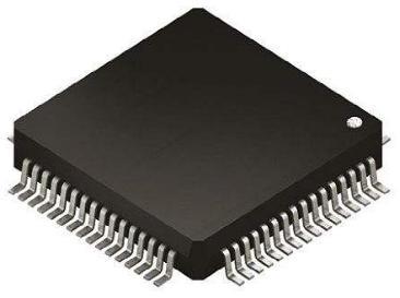
Figure 2 QFP package diagram
三、BGA type package
With the development of integrated circuit technology, the packaging requirements of the integrated circuit more stringent. This is because the packaging technology is related to the functionality of the product. When the frequency of the IC exceeds 100MHZ, the traditional encapsulation method may produce the so-called "CrossTalk" phenomenon, and when the number of pins of the IC is greater than 208 Pin, the traditional packaging Its difficulty. Therefore, in addition to the use of QFP package, the majority of today's high-foot chip are used to use BGA (BALL Grid Array PACKAGE) packaging technology.
BGA package has the following characteristics:
1、although the number of I / O pin increases, but the distance between the pins much larger than the QFP package, improve the yield.
2、BGA array of solder ball and the substrate contact surface large and short, is conducive to heat.
3、BGA array solder ball pin is short, shorten the signal transmission path, reducing the lead inductance, resistance; signal transmission delay is small, greatly improve the frequency of adaptation, which can improve the performance of the circuit.
4、assembly can be used coplanar welding, reliability greatly improved.
5、BGA for MCM package, can achieve high density MCM, high performance.
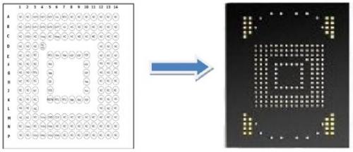
Figure 3 BGA package diagram
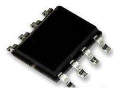
四、SO type package
SO type package includes: SOP (small outline package), TOSP (thin outline package), SSOP (reduced SOP), VSOP (very small outline package), SOIC (small outline integrated circuit package) and other similar to the QFP form The package is only available on both sides of the pin-in-chip package, one of which is one of the surface-mount packages, and the leads are drawn "L" on both sides of the package. The typical characteristics of this type of package is to make a lot of pins around the package, the package is easy to operate, the reliability is relatively high, is one of the current mainstream packaging, the more common is used in some memory type IC.
五、QFN package type
The QFN is a leadless quad flat package that is a lead-free package with a peripheral pad and a chip pad for mechanical and thermal integrity exposure. The package may be square or rectangular. Four sides of the package are equipped with electrode contacts, due to no lead, the placement area is smaller than the QFP, the height is lower than the QFP.
QFN package features:
1、 surface mount package, no pin design;
2、no lead pad design occupies a smaller PCB area;
3、the components are very thin (<1mm), to meet the stringent requirements of space applications;
4、very low impedance, self-inductance, to meet the high-speed or microwave applications;
5、with excellent thermal performance, mainly because the bottom of a large area of thermal pad;
6、light weight, suitable for portable applications.
QFN package for small form factor features, can be used for notebook computers, digital cameras, personal digital assistants (PDA), mobile phones and MP3 and other portable consumer electronics products. From the market point of view, QFN package more and more by the user's attention, taking into account the cost, volume of various factors, QFN package will be the next few years a growth point, the development prospects are extremely optimistic.
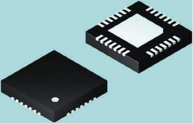
Figure 5 BGA package diagram
六、 PLCC package type
PLCC is a lead-on plastic chip package. The surface mount type of package, the pin from the four sides of the package leads, was "small" shape, dimensions smaller than the DIP package. PLCC package suitable for SMT surface mount technology to install wiring on the PCB, with small size, high reliability advantages. PLCC is a special pin chip package, which is a kind of Amotech chip package, this package pin inward at the bottom of the chip bending, so the chip in the top view is not see the chip pin. The welding of this chip using reflow process, the need for special welding equipment, in the debugging to remove the chip is also very troublesome, and now has been rarely used.
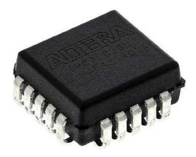
Figure 6 PLCC package diagram
As the IC package type, for the R & D test, little effect, but for the factory mass production burning, IC packaging type more, then select the corresponding supporting the burner model will be more. ZLG Zhiyuan Electronics for more than 10 years specializing in chip burning industry, its programmer to support and provide a variety of packaging type IC burner, for factory mass production.
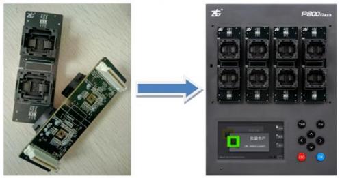
Figure 7 P800Flash programmer